Abstract
Thin films of copper nickel oxide (CuNiO2) were prepared by thermal oxidation of metallic copper nickel film formed by DC magnetron sputtering of quimolar Cu50Ni50 target. The as-deposited copper nickel films were thermally oxidized in oxygen atmosphere at different temperatures in the range 250-350oC. The as-deposited and oxidized films were characterized for their chemical composition, structure and surface morphology, electrical and optical properties. The films oxidized at 350oC were of CuNiO2 with polycrystalline nature and crystallite size of 38 nm. The influence of oxidation temperature on the physical properties was systematically investigated. The films oxidized at temperature of 350oC were CuNiO2with electrical resistivity of 7 Ωcm and optical band gap of 2.50 eV.
Key words
Copper nickel oxide; DC Magnetron Sputtering; Structure, Electrical resistivity: Optical absorption.
Introduction
Cuprous oxide is a p-type semiconducting oxide material finds potential applications in the field of gas sensor, solar cells, electro-chromic devices and p- type transparent conductive coatings. Doping of nickel into copper oxide modifies the electrical properties by introducing acceptor levels in copper oxide [1]. CuO-NiO mixed metal oxide nanoparticles are potential as a catalyst for various organic reactions such as methanol synthesis and humidity and non-enzymatic glucose sensors [2-4]. Copper nickel oxide in thin film form find applications as NO2 gas sensor, anode for fuel cells, solar selective coatings, solar cells, electrochromic devices, light emitting diodes, photodiodes, p-type gate in heterojunction field effect transistors, p-type transparent conducting coatings, antifungal coatings and super-capacitor coatings [5-19]. CuxNi1-xOthin films with different copper compositions were deposited by various methods such as spray pyrolysis, sol-gel process electro-deposition, pulsed laser deposition, pulsed plasma deposition, co-evaporation, DC magnetron sputtering and RF magnetron sputtering [6-12,14,16,17,19-35]. In the literature, Yang et al. [27] reported that the p-Cu0.1Ni0.9O thin films formed by pulsed plasma deposition showed the electrical resistivity of 0.19 Ωcm and optical band gap of 3.7 eV. Miyata et al. [31] noticed the electrical resistivity increased from 96 to 8x10⁵Ωcm and optical bands gap increased from 2.6 to 3.9 eV with increase of nickel content in RF reactive magnetron sputtered CuNiO (Ni = 0 -100 at.%) films. Elsayed et al. [14] formed nanocrystalline CuNiO2 films by sol-gel process with optical band gap of 2.4 eV. The electrical resistivity of 27 Ωcm and optical band gap of 2.0 eV were obtained by RF magnetron sputtering by using equimolar Cu50Ni50 target [34]. Menaka et al. [22] deposited CuxNi1-xO (x = 0.02 – 0.08) films by spray pyrolysis and noticed that the electrical resistivity decreased from 250to 88 Ωcm and optical band gap decreased from 3.94 to 3.58 eV with increase of copper content from 2 to 8 at.% respectively. In the present investigation, an attempt is made in the preparation of copper nickel oxide (CuNiO2) thin films by thermal oxidation of metallic CuNi thin films formed by DC magnetron sputtering method. The thermally oxidized CuNiO2 thin films were characterized for their composition, structure, electrical and optical properties.
Experimental
Thin metallic CuNi films were deposited by employing DC magnetron sputtering technique using the composite target of Cu50Ni50 (99.95% purity) with 50 mm diameter. The sputter chamber was evacuated to achieve the ultimate pressure of 1x10⁻⁵mbarusing diffusion pump backed by rotary pump. Pressure in the sputter chamber was measured with Pirani and Penning gauges. Before introducing the glass substrates in sputter chamber, the substrates were cleaned with degreasing solution followed by washing in deionized water. Later, the substrates were immersed in potassium dichromate solution for an hour and finally cleaned ultrasonically in a stainless steel tank for 15 minutes and dried with flow of nitrogen gas then transferred into chamber for deposition of copper nickel thin films. Target to substrate distance maintained was 50 mm. After achieving the ultimate pressure, argon gas was admitted into the sputter chamber through fine controlled needle valve to achieve sputter pressure of 3x10⁻²mbar. The films were deposited on glass substrate held at room temperature and the DC power fed to the sputter target was 90 W. The duration of the deposition of the film was 10 min. As-deposited metallic CuNi films were thermally oxidized in oxygen atmosphere for three hours in the temperature (Ta) range 250oC to 350oC in order to transform in to copper nickel oxide films. The as-deposited and thermally oxidized films were characterized for their chemical composition, structure and surface morphology, electrical and optical properties. Thickness of the deposited CuNi film determined with Veeco Dektak (Model 150) was 220 nm. Chemical composition of the metallic and oxide films was determined with energy dispersive X-ray analysis (EDAX) (Oxford instruments Inca Penta FETX3). Ccrystallographic structure of the films was determined with X-ray diffraction (XRD) (RigakuMiniflexII) X-ray diffractometer using copper Kα radiation with wavelength of 0.15406 nm. The surface morphology of the films was analyzed with atomic force microscope (AFM) (Seiko Instruments). Electrical resistivity, Hall mobility and carrier concentration were determined by using a Hall effect measurement system (ECOPIA HMS-3000 VER3.51.3). Optical transmittance of the films was recorded with Perken - Elmer double beam spectrophotometer in the wavelength range 300 - 800 nm in order to understand the optical absorption and to determine the optical band gap.The influence of oxidation temperature on the physical properties was systematically investigated on the copper nickel oxide films.
Results and discussion
Chemical composition
Chemical composition of the as-deposited metallic copper nickel films formed on silicon substrates and thermally oxidized copper nickel oxide films were analyzed with energy dispersive X-ray analysis. Figure 1a shows the EDAX spectrum of copper nickel films. The film showed the characteristic constituent peaks of copper and nickel. The chemical composition of the film was calculated from the intensities of copper and nickel peaks. The copper nickel film contained the copper content of 50.7 at. % and nickel 49.3 at. %. There was no peak related to oxygen which indicated that the as-deposited were of copper nickel films. The EDAX spectra exhibited that the intensity of oxygen peak increased with increase of oxidation temperature. It revealed that the oxidation of copper nickel films leads to transform into the copper nickel oxide. The increase in the intensity of characteristic peak of oxygen indicated the increase of oxygen content in the films due to convert into copper nickel oxide with the increase of temperature of oxidation as shown in figure1b, c, and d. The ratio of peak intensity of copper to nickel remains almost constant to unity. The chemical composition of the as-deposited and thermally oxidized films is given table 1. It is seen from the table that the content of oxygen in the films increased from 44.8 at. % to 49.4 at. % with increase of temperature from 250ºC to 350ºC respectively. It clearly indicated that the CuNi films oxidized at temperature of 350ºC were of stoichiometric CuNiO2.
Table 1. Chemical composition of copper nickel oxide films oxidized at different temperatures.
Film |
Oxidation temperature (oC) |
Chemical composition (at. %) |
Copper |
Nickel |
Oxygen |
CuNi |
As-deposited
250
300
350 |
48.9
28.2
26.9
25.0 |
51.1
26.9
25.8
25.6 |
----
44.8
47.3
49.4 |
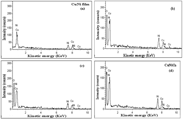
Figure 1. S Energy dispersive X-ray of (a) as-deposited copper nickel thin film and the films oxidized at temperatures: (b) 250ºC, (c) 300ºC and (d) 350ºC
It revealed that the temperature of 350ºC is an optimum to oxidize metallic copper nickel films into copper nickel oxide (CuNiO2).It is to be noted that CuNiO2 thin films were also achieved by RF reactive magnetron sputtering of equimolarCu50Ni50 target at an oxygen partial pressure of 2x10⁻⁴ mbar [34].
Structural Properties
X-ray diffraction profile of as-deposited copper nickel film is shown in figure 2. The diffraction pattern of the films was polycrystalline nature. The film exhibited weak diffraction peaks at 22.1º, 29.2º and strong peaks at 37.4º, 44.2ºand 51.3º. A weak peak located at 22.1º was related to the (200) reflection of NiO [36,37]. Another diffraction reflection seen at 29.2º related to copper nickel / Cu2O [38,39]. The peak seen at 37.4º corresponds to the (222) reflection of NiO and the peaks situated at 44.2ºand 51.3º were connected to the CuNi alloy [7,40]. It revealed that the as-deposited film was of CuNi along with traces nickel oxide. The presence of nickel oxide phase and copper oxide was mainly due to the oxidation of nickel and copper with residual oxygen in the sputter chamber during the growth of the films. Figure 2 shows the X-ray diffraction profiles of thermally oxidized copper nickel oxide films at temperatures of 250ºC, 300ºC and 350ºC. It is seen from the diffraction profiles that the thermally oxidized films were also of polycrystalline in nature. The films oxidized at 250ºC showed the X-ray diffraction peaks at 37.1º and 43.9º related to the (111) and (200) reflections of CuNiO2 [27]. As the oxidation temperature increased to 300ºC the intensity of diffraction peaks increased which indicated the improvement in the crystallinity of the films. Further increase of oxidation temperature to 350ºC, there was enhancement in the peak intensities of (111) and (200) along with the appearance of diffracted peak at 41.4º related to the (002) reflection of CuNiO2. From the X-ray diffraction peaks the interplanar distance and the lattice parameters were calculated. The structure of the films oxidized at temperature of 350oC was tetragonal with lattice parameters, a = 0.4112 nm and c= 0.4361 nm. The given thermal energy to the copper nickel films in presence of oxygen leads to transform the copper nickel films into copper nickel oxide. It revealed that the increase of oxidation temperature to 350ºC the metallic copper nickel films were transformed into CuNiO2 with enhanced crystallinity. The crystallite size (D) of the as-deposited and thermally oxidized films was calculated from the full width at half maximum intensity (β), the diffraction angle (θ) of the (111) peak, and the wavelength of copper X-rays using Debye-Scherrer’s relation [41]
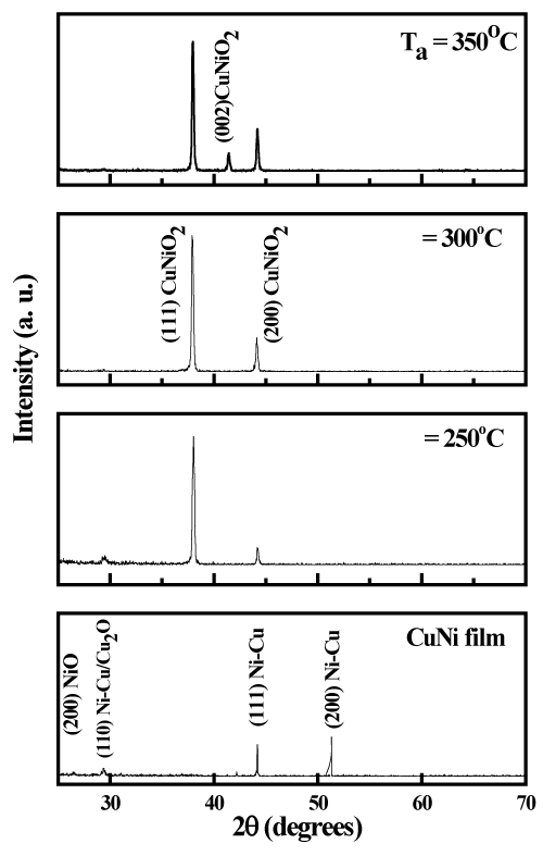
Figure 2. X-ray diffraction profiles of (a) as-deposited copper nickel film and thermally oxidized copper nickel oxide films: (b) 250ºC, (c) 300ºC and (d) 350ºC.
D = Kλ / βcosθ ----- (1)
where K is a constant with a value of 0.89 for X-ray target of copper and θ the diffraction angle. The full width at half maximum intensity of peak decreased with increase of oxidation temperature which indicated the crystallite size increased with the oxidation temperature. The crystallite size of the as-deposited copper nickel film was 13 nm. As the temperature of oxidation increased to 350ºC the crystallite size increased to 38 nm as shown in figure 3. It was reported low crystallite size of 32 nm in spray deposited copper nickel oxide films [21]. The dislocation density (δ) of the films was determined from the crystallite size using the relation [42].
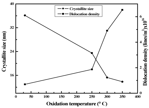
Figure 3. Variation in Crystallite size and dislocation density of copper nickel oxide films with oxidation temperature.
δ = 1/D2 ----- (2)
The dependence of dislocation density on the oxidation temperature of the films are shown in figure 3. The dislocation density of the as-deposited metallic copper nickel film was 7.5x10¹⁶ lines/m2. As oxidation temperature increased the dislocation density decreased to 4.1x10¹⁶ lines/m2 in copper nickel oxide films oxidized at temperature of 300ºC. Further increase of oxidation temperature to 350oC the dislocation density decreased to 1.2x10¹⁶ lines/m2. The low value of dislocation density in the CuNiO2 films oxidized at higher temperature was mainly due to the larger crystallite size. It is to be noted that the dislocation density reported in the CuNiO2 films was high value of 15x1016 lines/m2 in bias magnetron sputtered CuNiO2 films [34]. The strain (ε) developed in the films was calculated from the X- ray diffraction peak and full width at half maximum intensity using the relation [43].
ε = β cosθ / 4 ----- (3)
Figure 4 shows the dependence of strain on the oxidation temperature of the copper nickel oxide films. It is seen from the figure that the strain in the metallic copper nickel films was 9.4x10⁻⁴ lines-2/m4. The strain in the films decreased with oxidation temperature. The films oxidized at 250oC exhibited the strain of 7.4x10⁻⁴ lines-2/m4.The number of crystallites (N) were calculated from the crystallite size and thickness of the film using the relation [44].
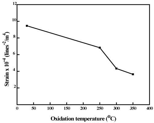
Figure 4. Dependence of strain on the thermal oxidation temperature of copper nickel oxide films.
N = t/D3 ----- (4)
The number of crystallites in metallic CuNi films 0.100 nm-2. In the case copper nickel oxide films the number of crystallites decreased from 0.037 to 0.004 nm-2 with increase of oxidation temperature from 250oC to 350oC respectively.
Surface Morphology
Atomic force microscope was used to analyze the surface morphology of as-deposited CuNi films and thermally oxidized copper nickel oxide films. Figure 5 shows the three dimensional and two dimensional atomic force micrographs of as-deposited copper nickel (figure 5a), thermally oxidized copper nickel oxide films (figure 5b, c, and d) respectively. As-deposited films were of fine grain structure while those oxide films were of larger in grain size. The variation ingrain size with the oxidation temperature of CuNiO2 films is shown in figure 6.The grain size of the as-deposited copper nickel films was 55 nm. As the oxidation temperature increased, the thermal energy accelerates the coalescence of small grains into larger ones, and also reacts with oxygen to form copper nickel oxide. The grown grains were of almost spherical in shape. The root mean square (RMS) roughness of the metallic CuNi films was 2.0 nm. In copper nickel oxide films oxidized at temperature of 350ºC of high roughness of 12.1 nm as shown in figure 6. Such an increase in the roughness with deposition temperature was notices in aluminum oxide thin films formed by DC magnetron sputtering [45] and Cu2O films deposited by DC magnetron sputtering [46].
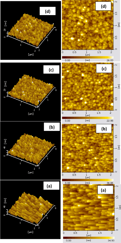
Figure 5. Two and Three dimensional AFM images of (a) copper nickel film and copper nickel oxide films oxidized at temperatures: (b) 250ºC, c) 300ºC and (d) 350ºC.
Electrical Properties
The electrical properties of the films are strongly influenced by the oxidation temperature. The dependence of electrical resistivity on the oxidation temperature of copper nickel oxide films is shown in figure 7. Electrical resistivity of metallic copper nickel films was 4x10⁻³ Ωcm. As the temperature increased the oxidation of copper nickel films was takes place. The films oxidized at 250ºC were partially oxidized and showed the electrical resistivity of 5x10⁻¹ Ωcm. Further increase of oxidation temperature to 350ºC the films were fully oxidized and form CuNiO2. These oxide films showed the electrical resistivity of 7 Ωcm. The oxide films are in general of high electrical resistivity when compared to mixed phase oxide films. In the literature, it was reported that the electrical resistivity in pulsed laser deposited Ni0.9Cu0.1O films was 0.19 Ωcm [27]. Miyata et al. [31] achieved electrical resistivity of 70Ωcm and 4x10⁴Ωcm in RF magnetron sputtered Cu2O and NiO films respectively, while equimolar Cu-Ni oxide films showed the value of 2x10⁴ Ωcm. Chen et al. [32] reported low electrical resistivity of 36 Ωcm in 9 at. % copper doped nickel oxide films. The variation in the electrical resistivity of the copper nickel oxide films was mainly due to the difference in the chemical composition and the deposition method of the films. Hall effect measurements indicated that the metallic copper nickel films were of n- type while copper nickel oxide films were of p-type in electrical conduction. When the films oxidized the type of charge carrier transport changed from electronic to hole conduction. Figure 8 shows the variation of Hall mobility of the copper nickel oxide films with the oxidation temperature. The metallic copper nickel films showed electron mobility of 0.4 cm2/V.sec. As the oxidation temperature increased the hole mobility increased from 3.1 cm2/V.sec and reached a value of 7.8 cm2/V.sec with increase of oxidation temperature from 250ºC to 350ºC in CuNiO2 films. The electron concentration in metallic copper nickel film was 3.9x1018 cm-3. Hole concentration in the films decreased from 4.0x10¹⁷ to 1.1x1016 cm-3 with increase of oxidation temperature from 250ºC to 350ºC respectively as shown in figure 8. Miyata et al. [31] reported low Hall mobility of 2 cm2/V.sec and low carrier concentration of 8x1013 cm-3 due to high electrical resistivity of copper nickel oxide films. In contrast to this, Chen et al. [32] obtained Hall mobility of 1 cm2/V.sec and carrier concentration of 2x1020 cm-3 in 18 at. % of copper doped NiO films formed by RF magnetron sputtering.
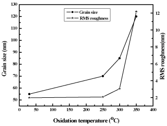
Figure 6. Variation in Grain size and root mean square roughness of copper nickel oxide films with oxidation temperature.
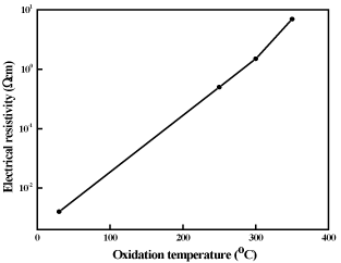
Figure 7. Dependence of electrical resistivity on oxidation temperature of copper nickel oxide films.
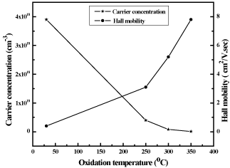
Figure 8. Variation in Carrier concentration and Hall mobility of copper nickel films with oxidation temperature.
Optical Properties
Optical transmittance of metallic copper nickel and thermally oxidized copper nickel oxide films was recorded in order to study the optical absorption and to determine the optical band gap. Figure 9 shows the optical transmittance spectra of copper nickel and copper nickel oxide thin films oxidized at different temperatures. It is seen from the figure that the transmittance of copper nickel thin film was very low (< 3%) since the metal films reflect the incident radiation. As the oxidation temperature increased to 250ºC the transmittance of the films increased and showed about 19% (at wavelength of 600 nm). This is due to partially oxidation of CuNi films in to copper nickel oxide. Further increase of oxidation temperature to 350ºC the transmittance enhanced to about 30 % due to the formation of copper nickel oxide films. The fundamental optical absorption edge of the films shifted towards lower wavelength side with increase of oxidation temperature. Absorption coefficient (α) of the films calculated from the thickness of the film (t) and optical transmittance (T) data using the relation.
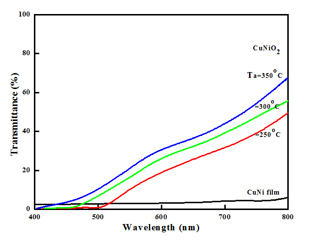
Figure 9. Optical transmittance spectra of thermally oxidized copper nickel oxide films.
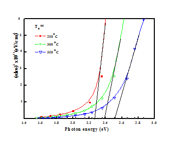
Figure 10. Plots of (αhυ)2 versus photon energy of copper nickel oxide films.
α = - (1/t) ln T ----- (5)
The optical band gap (Eg) of the films was determined from the absorption coefficient and the photon energy using Tauc’s relation [47] assuming the direct transitions take place from the top of the valence band to the bottom of conduction band.
(αhν) = A (hν - Eg) ½ ----- (6)
Figure 10 shows the plots of (αhν)2 versus photon energy (hν) of the copper nickel oxide films oxidized at different temperatures. By extrapolating the linear portion of the plots to α = 0 resulted the optical band gap. Optical band gap of the films increased from 2.25 to 2.50 eV with increase of oxidation temperature from 250ºC to 350ºC respectively. Summary of the electrical and optical properties of copper nickel oxide films of different compositions formed by various deposition techniques are given in table. The low value of optical band gap of the films oxidized at low temperatures was mainly due to the partial oxidation of the films. It is to be noted that the optical band gap of 50% Cu in copper nickel oxide films was 2.75 eV in RF magnetron sputtered and 3.04 eV in spray deposited films [20,31]. It is to be noticed that the optical band gap of 2.0 eV was obtained in RF magnetron sputtered and 2.4 eV in sol-gel processed CuNiO2 films. It is seen from the table that the large variations in the electrical resistivity and optical band gap depends on the deposition method and deposition parameter [14,30]. The low electrical resistivity and small band gaps were due to the mixed phase films.
Table 2. Summary of electrical and optical properties of Cu-Ni-O films prepared by different methods.
S.No.
|
Deposition method |
Target
composition
|
Film
composition |
Substrate temperature/ Annealing temperature (ºC) |
Electrical resistivity
(Ωcm) |
Optical bandgap (eV) |
Ref. |
1 |
Spray pyrolysis |
--
|
CuxNi1-xO
(x=0- 0.10) |
350
|
---
|
3.2 -2.96 |
20 |
2 |
Spraypyrolysis |
-- |
CuxNi1-xO
(x = 0.02-0.08) |
450 |
3
250 - 88 |
3.94-3.58 |
22 |
3 |
Sol-gel process |
--- |
CuNiO2 |
150 |
--- |
2.4 |
14 |
4 |
Sol-gel process |
--- |
Cu0.05Ni0.95O
|
550 |
0.23 |
3.69 |
24 |
5 |
RF Magnetron sputtering |
Cu:NiO
(Cu=0-9.8%) |
Cu-Ni-O |
100 |
8.7 |
3.3 |
17 |
6 |
RF magnetron sputtering
|
CuO-NiO
Cu= 0-100%) |
Cu-Ni-O |
30 |
70-4x10⁴ |
2.6 -3.9 |
31 |
7 |
RF magnetron sputtering |
NiO-Cu |
Cu0.09Ni0.91O
|
30 |
36 |
--- |
32 |
8 |
RF magnetron sputtering |
Cu50Ni50
|
CuNiO2 |
250 |
27 |
2.0 |
33 |
9 |
RF Magnetron sputtering |
CuO : NiO
(0.18:0.82) |
Cu-Ni-O |
30 |
0.12 |
2.41 |
35 |
10 |
RF Magnetron sputtering |
Cu:NiO
(Cu=0-12%) |
Cu-Ni-O |
30 |
----- |
3.86 - 3.63 |
38 |
11 |
Pulsed plasma deposition
|
NiO-CuO |
Cu0.1Ni0.9O
|
30 |
0.19 |
3.7 |
27 |
12 |
DC magnetron sputtering |
Cu0.3Ni0.7
|
Cu0.3Ni0.7O
|
100 |
81 |
2.2 |
29 |
13 |
DC magnetron sputtering |
Cu50Ni50
|
CuNiO2 |
250 - 350 |
0.5 – 7.0
-7 |
2.25 -2.50 |
Present
work |
Conclusions
Thermal oxidation process was employed for the growth of copper nickel oxide thin films. Metallic copper nickel films were deposited by DC magnetron sputtering of equimolar target of Cu50Ni50 on to glass substrates held at room temperature. As-deposited copper nickel film was thermally oxidized in oxygen atmosphere at different temperatures in the range 250 – 350oC. These films were characterized for chemical composition, structure, electrical and optical properties. The films oxidized at temperatures less than 350oC were deficiency in the oxygen content where as those oxidized at 350oC were of CuNiO2. These CuNiO2 films were of polycrystalline in nature with tetragonal structure with crystallite size of 38 nm. The electrical resistivity of the films decreased with increasing of oxidation temperature and exhibited a value of 7 Ωcm. Hall effect studies indicated that the oxide films were of p-type in electrical conduction with Hall mobility of 7.8 cm‑/V.sec. The optical absorption edge shifted towards lower wavelength side with increase of oxidation temperature. Optical band gap of the CuNiO2 films oxidized at temperature of was 2.25 eV.
Acknowledgement
K. Ravindra is thankful to the University Grants Commission (UGC), New Delhi, India for the award of Junior Research Fellowship under UGC-BSR-RFSMS Fellowship Programme and Dr. S. Uthanna is thankful to the University Grants Commission, New Delhi for the award of UGC-BSR- Faculty Fellowship.
References
- Martinez-Ruiz A, Moreno MG, Takeuchi N (2003) First principles calculations of the electronic properties of bulk Cu2O, clean and doped with Ag, Ni and Zn. Solid State Sci 5: 291-295.
- Meloni D, Monaci R, Solinas V, Auroux A, Dumitriu E (2008) Characterization of the active sites in mixed oxides derived from LDH precursors by physicochemical and catalytic techniques. Appl Catal A 350: 86-95.
- Jeseentharani V, Jeyaraj B, Pragasam J, Dayalan A, Nagaraja KS (2010) Humidity sensing properties of CuO, ZnO and NiO composites. Sens Transducers J 113: 48-55.
- Cao F, Guo S, Ma H, Yang G, Yang S, et al. (2011) Highly sensitive nonenzymatic glucose sensor based on electrospun copper oxide-doped nickel oxide composite microfibers. Talanta 86: 214-220. [Crossref]
- Banno S, Imanaka N, Adachi G (1995) Selective nitrogen dioxide sensor based on nickel copper oxide mixed with rare earths. Sens Actuators B 24-25: 619-622.
- Shobha T, Aravinda CL, Gomathi Devi L, Mayanna SM (2003) Preparation and characterization of oxides of Ni-Cu: anode material for methanol oxidative fuel cells. Solid State Electron 7: 451-455.
- Aravinda CL, Mayanna SM, Bera P, Jayaram V, Sharma AK (2002) XPS and XAES investigations on electrochemically deposited Cu-Ni solar selective back coatings on molybdenum substrate. J Mater Sci Lett 21: 205-208.
- He Z, Ji Z, Zhao S, Wang C, Liu K, et al. (2006) Characterization and electrochromic properties of CuxNi1-xO films prepared by sol-gel dip-coating. Solar Energy 80: 226- 230.
- Sonavane AC, Inamdar AI, Shinde PS, Deshmukh HP, Patil PS (2010) Efficient electrochromic nickel oxide thin films by electrodeposition. J Alloys Compd 489: 667-672.
- Zhao L, Su G, Liu W, Cao L, Wang J, et al. (2011) Optical and electrochemical properties of Cu-doped NiO films prepared by electrochemical deposition. Appl Surf Sci 257: 3974-3979.
- Yuan G, Liu Y, Yue M, Li H, Liu E, et al. (2014) Cu-doped NiO for aqueous asymmetric electrochemical capacitors. Ceram Int 40: 9101-9105. [Crossref]
- Yin JL, Park JY (2014) Electrochemical investigation of copper/nickel oxide composites for supercapacitor applications. Int J Hydrogen Energy 39: 16562-16568.
- Chan IM, Hsu TY, Hong FC (2002) Enhanced hole injections in organic light emitting devices by depositing nickel oxide on indium tin oxide anode. Appl Phys Lett 81: 1899-1903.
- Elsayed IA, Cava M, Gupta RK, Fahmy T, Al- Ghandi A, et al. (2015) Photoconducting and photcapacitance properties of Al/p-CuNiO2/p-Si isotype hetero-junction photodiode. J Alloys Compd 638: 166-171.
2021 Copyright OAT. All rights reserv
- Greco G, Fioreng P, Raineri V, Malandrino G, Nigro RI (2012) Epitaxial NiO gate dielectric on AlGaN/GaN heterostructures. Appl Phys Lett 100: 063511.
- Chen SC, Kuo TY, Jen SU, Chiang HP, Liu WY, et al. (2015) Effect of copper content on the electrical stability of nickel oxide films. Thin Solid Films 584: 238-242.
- Sato K, Kim S, Komuro S, Zhao X (2016) Characteristics of Cu-doped amorphous NiO films formed by RF magnetron sputtering. Jap J Appl Phys 55: 06GJ10.
- Rahdar A, Aliahmad M, Azizi Y, Keikha N, Moudi M, et al. (2017) CuO-NiO Nano composites: Synthesis, characterization and cytotoxicity evaluation. Nanomed Res J 2: 78-86.
- Zhang L, Gong H (2017) Unraveling the correlation between nickel to copper ratio of binary oxides and their superior supercapacitor performance. Electrochemica Acta 234: 82-92.
- Moghe S, Acharya AD, Panda R, Shrivastava SB, Gangrade M, et al. (2012) Effect of copper doping on the change in the optical absorption behaviour in NiO thin films. Renewable Energy, 46: 43-48.
- Abbass KH (2015) Spray pyrolysis deposition and effect of annealing temperature on optical properties of Cu:NiO Film. Int Lett Chem Phys Astronomy 47: 178-184.
- Menaka SM, Umadevi G, Manickam M (2017) Effect of copper concentration on the physical properties of copper doped NiO thin films deposited by spray pyrolysis. Mater Chem Phys 191: 181-187.
- Gowthami V, Meenakshi M, Anandhan N, Sanjeevaraja C (2014) Preparation of Cu-doped nickel oxide thin films and their properties. AIP Cong Proc 1591: 884-885.
- Kim KH, Takahashi C, Abe Y, Kawamura M (2014) Effect of Cu doping on nickel oxide thin film prepared by sol-gel solution process. Optik 125: 2899-2901.
- Zhang L, Tang C, Gong H (2014) Temperature effect on the binder-free nickel copper oxide nanowires with superior supercapacitor performance. Nanoscale 6: 12981-12989. [Crossref]
- Kikuchi N, Tonooka K, Kusano E (2006) Mechanisms of carrier generation and transport in Ni-doped Cu2O.Vacuum 80: 756-760.
- Yang M, Shi Z, Feng J, Pu H, Li G, et al. (2011) Copper doped nickel oxide transparent p-type conductive thin films deposited by pulsed plasma deposition. Thin Solid Films 519: 3021-3025.
- Potzelberger I, Mardare AI, Hassel AW (2017) Non-enzymatic glucose sensing on copper-nickel thin film alloy. Appl Surf Sci 417: 48-53.
- Ashok Kumar Reddy Y, Sivasankar Reddy A, Sreedhara Reddy P (2013) Influence of oxygen partial pressure on the structural, optical and electrical properties of Cu-doped NiO thin films. Phys Scripta 87: 015801.
- Burgstaller W, Hafner M, Voith M, Mardare AI, Hassel AW (2014) Copper-nickel oxide thin film library reactively co-sputtered from a metallic sectioned cathode. J Mater Sci 29: 148-157.
- Miyata T, Tanaka H, Sato H, Minami T (2006) p-type semiconducting Cu2O-NiO thin films prepared by magnetron sputtering. J Mater Sci 41: 5531-5537.
- Chen SC, Kuo TY, Lin YC, Lin HC (2011) Preparation and properties of p-type transparent conductive Cu-doped NiO films. Thin Solid Films 512: 4944-4947.
- Sreedhar A, Hari Prasad Reddy M, Uthanna S, Pierson JF (2013) Sputter power influenced structural, electrical and optical behaviour of nanocrystalline CuNiO2 films formed by RF magnetron sputtering. ISRN Cond Mater Phys Volume 2013: Article ID 527341.
- Sreedhar A, Hari Prasad Reddy M, Uthanna S, Pierson JF (2013) Structural and electricalcharacteristics of nanocrystalline copper nickel oxide films formed by RF magnetron sputtering. Phys Exp 3: 15.
- Chen WY, Jeng JS, Huang KL, Chen JS (2013) Modulation of Ni valence in p-type NiO films via substitution of Ni by Cu. J Vac Sci Technol A 31(2): 021501.
- Taguchi H (1998) Relation between crystal structure and electrical properties of murdochite-type Ni6+2xMn1-xO8 Solid State Commun 108: 635-639.
- JCPDS International Centre for Diffraction Data Card No. 89-5881.
- Manouchehri I, Mehrparvar D, Moradian R, Gholami K,Osati T (2016) Investigation on structural and optical properties of copper doped NiO thin films deposited by RF magnetron reactive sputtering. Optik 127: 8124-8129.
- Ng SC, Brockhouse BN, Hallman ED (1967) Characterization large alloy single crystals byneutron diffraction. Mater Res Bull 2: 69-73.
- JCPDS International Centre for Diffraction Data Card No. 06-0720.
- Cullity BD, Elements of X-ray Diffraction, 2ndEdn, Addison Wesley (1978).
- Singh I, Bedi BK (2011) Studies and correlation among the structural, electrical and gas response properties of aerosol spray deposited itself assembled nanocrystalline CuO. Appl Surf Sci 257: 7592.
- Williams JB, Hallman RC (1981) Phil Mag 3:211.
- Shrividhya T, Ravi G, Hayakawa Y, Mahalingam T (2014) Determination of structural and optical parameters of CuO thin films prepared by double dip technique. Mater Electron 25: 3885-3894.
- Sivasankar Reddy A, Venkata Rao G, Uthanna S, Sreedhara Reddy P (2006) Structural and optical studies on dc reactive magnetron sputtered Cu2O films. Mater Lett 60: 1617.
- Alexandrescu R, Morgan I, Voicu I, Pugna G, Petcu S, et al. (1997) J Phys D: Appl Phys 30: 2620.
- Tauc J (1974) Amorphous and Liquid Semiconductors; Plenum Press, New York.