Hexagonal nanostructures were prepared from the reaction of a phosphorus film with Sn/SnI4 at 650 °C under a pressure of 250 psi to 600 psi. The hexagons are composed of Sn and P in a proportion of 1:1 and contain cage tubes that are parallel to each other. The film temperature, pressure, and reaction time can affect the formation of the fine hexagonal nanostructures. The SnP hexagon has a different morphology from that of the SnP reported. It also contains tubes of cage clusters, which are 4.22 Å apart.
Several allotropic forms of phosphorus exist, including white, red, and black. The white/yellow form of phosphorus exists as P4 molecules and is quite reactive when exposed to air due to rapid oxidation. Red phosphorus (RP) is comprised of five different forms of covalently bonded phosphorus atoms, namely types I to V, all of which exhibit a reddish color and exist as amorphous to crystalline forms. Type I is amorphous RP while types II and III have not yet been fully characterized and there is no information about their crystal structures in the literature. RP types IV and V (most commonly known as fibrous phosphorus and violet phosphorus, respectively) have been fully characterized and their crystal structures can be found elsewhere [1-3]. Black phosphorus (BP) is a stable, semiconducting allotrope of phosphorus [4,5] that was first discovered by Bridgman in 1914 [6]. Recently, Lange et al. found that BP could be grown from red phosphorus at 873K in a sealed ampoule in the presence of tin and tin (IV) iodide (SnI4) at a pressure as low as around 100 psi [7,8]. Recently, researchers are taking inspiration and insights from graphene and applying it to new or recently rediscovered 2D black phosphorus material [9-11].
Phosphorus reacts with many metals to form phosphides that have various structures. The simplest form of phosphides are binary phosphides containing P3- anion. Polyphosphides include P-P bonds and consist of clusters of phosphorus [12], such as P42-, P73-, P144- so the phosphorus atoms in polyphosphides have a range of negative charges. Phosphides and polyphosphides are generally prepared from reactions of metals and RP in the gas phase, or of metal salts with RP in solution [13]. Phosphides have been shown to be more stable than phosphorus allotropes when used in electronic or optoelectronic devices [14]. Bulky crystals of phosphides are typically obtained through the vapor transport process with the use of evacuated ampoules. Nano- to microscale particles of phosphides have been obtained via ionothermal synthesis [15] or ball milling [16] methods. However, few single crystal phosphide nanomaterials have been reported.
In this paper, we report the synthesis and characterization of a unique hexagonal SnP nanostructures using a two-step process which requires the deposition of a phosphorus thin film on a substrate, followed by a high temperature and high-pressure process in a pressure vessel.
Synthesis
RP powder (EMD Millipore), and tin (Fisher Scientific, 200 mesh) were used as received; Tin (IV) iodide was prepared using standard literature procedures [17]. Pressure vessel reactions were carried out in attempts to grow crystals from thin films of red phosphorus. First, amorphous red phosphorus powder was deposited on a Si/SiO2 with Au predeposited pads substrate using the chemical vapor deposition (CVD) technique: 0.5-5 mg of amorphous red phosphorus powder was placed in a quartz tube in the presence of the substrate, the tube was then placed inside a tube furnace and slowly heated up to 600°C under vacuum until all the red phosphorus sublimated and deposited on the substrate in the colder area inside the tube (Figure 1a). In the second step, the substrate containing the amorphous red phosphorus thin film was allowed to cool down to room temperature and then inserted in a 12 mL Pyrex tube or a Kimble conical-bottom glass centrifuge tube (Fisher Scientific) containing SnI4 and Sn. The Pyrex tube was placed in a 64 mm outer diameter and 11 mm wall thickness stainless steel pressure vessel (Pressure Product Industries) that was evacuated and backfilled 5x with argon (Airgas) to a variety of pressures (Figure 1b). No additional RP was added to the reaction vessel, thereby limiting the only source of RP to the film deposited on the substrate. The vessel was then secured in the tube furnace (Thermo Scientific) and heated up to the desired external temperature for the reaction to take place.
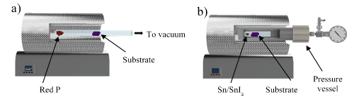
Figure 1. Schematic for growth of hexagonal tin/phosphorus structures. a) CVD technique procedure for the growth of thin red P films; b) Reaction of Sn/SnI4 with red P thin film under various pressures
After various temperatures ranging from 650 °C to 900 °C were applied in the presence of the Sn/SnI4 mixture during the second step in our two-step process, the structures of the products formed were investigated. The pressure vessel was placed inside a tube furnace and the temperature was raised to 650 °C, 700 °C, 800 °C, 850 °C, and 900 °C, respectively. The pressure vessel was run to one temperature and held for various times and then the tube furnace was turned off. Pressure conditions were also varied based on the starting pressure of the added argon with ranges from 250 psi to 500 psi. The starting point of 650 °C for the temperature range is not arbitrary, but is the temperature at which the conversion of BP in sealed ampoule reactions takes place [7,8,18]. Temperatures lower than this result in annealed red phosphorus products as investigated previously in sealed ampoule experiments [19]. Identical results were observed in our own studies as only red phosphorus was found to form with temperatures lower than this.
Characterization
Raman spectroscopy (Renishaw Ramascope RM-1000), scanning electron microscopy (SEM) (Hitachi TM-1000), transmission electron microscopy (TEM) (JEOL JEM2100), and power XRD (Rigaku SmartLab) were used for characterization of the crystalline hexagons. Selected Area Electron Diffraction (SAED) patterns were obtained at 120 kV on a TEM/STEM (JOEL JEM2100) equipped with an LaB6 electron gun. Energy Dispersive X-ray Spectroscopy data (EDS) were collected on the SEM instrument.
Formation of fine hexagonal nanostructures
At 650 °C, fine hexagonal structures were observed. Bright field images revealed a dense growth of nanostructures on the substrate surface (Figure 2a). SEM shows the phosphorus structures grew in the shape of hexagons. Figures 2b-d shows the morphological differences between the hexagon structures and the annealed film, suggesting a more crystalline material for the hexagons. The hexagons appeared in various thicknesses up to few microns and various diameters up to 9 µm. Holding the temperature at 650 °C for 18 hours brought about a higher concentration of these hexagons (Figure 2d). The structures grew in pressures ranging from 250-600 psi when the pressure vessel reached 650 °C. Control experiments run at 650 °C/250 psi in the absence of Sn or Sn/SnI4 showed various less-ordered shapes from annealed red phosphorus and no hexagons (Figure 3).
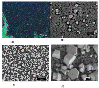
Figure 2. Images of red phosphorus film converted under 650 °C/250 psi in the presence of Sn/SnI4. (a) Brightfield images of dense region of phosphorus structures that grew on top of film. (b-d) SEM images of several areas of red phosphorus films converted under 650 °C/250 psi in the presence of Sn/SnI4. Annealed film following 6-hour reaction in b and c, and 18-hour in d
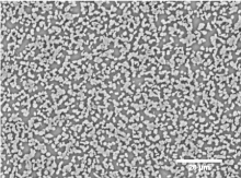
Figure 3. SEM images of control experiments run at 650 °C/250 psi in the absence of Sn, SnI4, or Sn/SnI4 showed random shapes from annealed red phosphorus
Conditions affecting the growth of hexagons
Temperature, pressure, and reaction time all play roles in the formation and the size of the hexagonal nanostructures. The hexagonal structures reported here only grow in a narrow T/P range (250 < P < 570 psi; 650 °C < T < 680 °C). Different structures with irregular shapes are formed when the temperature or pressure deviate from these ranges (Figure 4). To simplify the experiments and the number of independent reactions, two time intervals were used for the reaction, 6h and 18h (the time for which the reaction remained at the specified temperature). As mentioned in the last section, holding the temperature at 650 °C for 18 hours brought about a higher concentration of these hexagons and larger hexagons than those for 6 hours.
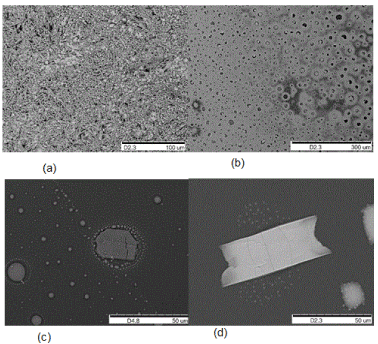
Figure 4. SEM images of products formed from red phosphorus films at various temperatures with an initial pressure of 500 psi for 6 hr. a) 700 °C; b) 800 °C; c) 850 °C; d) 900 °C
The substrate seems to have no significant effect on the formation and the shape of the hexagonal structures, since these hexagonal structures were also grown on Au- or Pt-coated SiO2 substrates such as pure SiO2 substrates and titanium foil. However, attempts to grow the hexagons onto a SiO2 substrate that is partially coated with Au brought about interesting results. A red phosphorus thin films were deposited onto a wafer that was partially coated with Au. When these were run under the same conditions, the hexagons were found to preferentially grow on the gold surface (Figure 5). The presence of gold also provided thinner hexagons when compared to performing the reaction on the SiO2 substrates. Average diameters were also larger for these samples (6 µm) with diameters reaching 10 µm for some samples, suggesting that the gold might provide a preferential surface for growth.
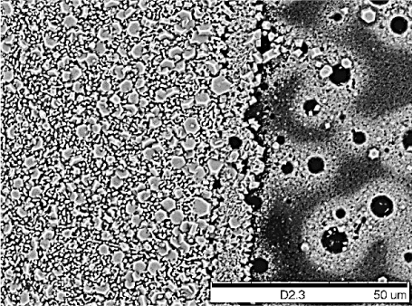
Figure 5. SEM images of red phosphorus films converted under 650 °C/250 psi after 18 hours. Preferential growth of the hexagons on gold (left half) compared to the SiO2
Characterization of the hexagons
Raman analysis of BP was first investigated experimentally by Sugai et al. [20] and computationally by Kaneta et al. [21]. Raman resonance spectroscopy quickly became a heavily used technique for the analysis of BP and RP [22]. As an aid in understanding the composition of these hexagons, Raman analysis was carried out on them. The Raman spectrum for the hexagon structures is shown in Figure 6 and the result is compared to those of BP and RP. The Raman spectrum shows three predominant bands located at 377 cm-1 and 411 cm-1 and 463 cm-1. Type I RP is amorphous. Crystalline structures of type II and III are not known so far. Both fibrous and violet forms of RP contain an arrangement of double tubes formed from the P8-P2-P9 cages as shown in Scheme 1 [19]. Both structures have the tubes with the primary difference being in their arrangement. The 377 cm-1 peak is likely the transverse breathing mode of the tube structures while the 411 cm-1 is likely corresponding to the longitudinal breathing modes of cage structures [19]. The fact that the 377 cm-1 is the most intense peak suggests that the P8 cages may predominantly be present. However, the Raman spectrum of the hexagons does not match with any of the RP forms. The Raman analysis verifies that these hexagons are not BP and also not any type of red phosphorus from types I to V, although P8 or P8-P2-P9 cage-like structures were observed. No Raman data on tin phosphides has been reported, so we could not conclude whether these hexagons are tin phosphides from the Raman analysis alone, therefore other analyses were conducted in order for us to understand the molecular structure of the hexagons.
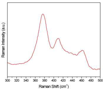
Figure 6. Raman spectrum of hexagon structures
The results from the Raman analysis are contradictory to the reports that fibrous and violet crystalline phosphorus nanowires can be synthesized by heating RP to a higher temperature in the presence of metal halides or a metal/metal halide combination [23]. The composition analysis of the sample is critical for understanding the molecular structure of the hexagons. Thus, SEM/EDS studies were carried out to obtain the composition of the hexagons. The SEM EDX analysis showed a 49.3/50.7% atom percentage ratio of P/Sn (Figure 7), suggesting a 1:1 ratio of P:Sn. The elemental map also indicated that the hexagons are made of P and Sn (Figure 8). This is not a surprise since phosphides can be prepared from reactions of metal or metal halides with red phosphorus [10].
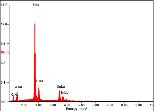
Figure 7. SEM/EDS data. The sample was on a SiO2/Si wafer
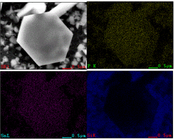
Figure 8. SEM Electron map of a hexagon on a SiO2/Si wafer
These hexagons are too small for a single-crystal X-ray diffraction analysis. Powder X-ray diffraction (XRD) experiments were conducted and the result is shown in Figure 9. D-spacing values of the hexagons are listed in Table 1 and compared to those of various RP allotropes and BP. These values do not match with BP or any RP allotropes [7,19]. The d-spacing values from XRD measured from the experimental results partially match with those of single crystal SnP reported by Gullman [24].
Table 1. X-ray powder spacing of hexagons, RP allotropes, BP, and tin phosphides. Unit: Å
Type II |
Type III |
Type IV |
Type V |
BP |
Sn4P3 |
SnP |
Hexagon |
|
|
|
10.7 |
|
|
|
|
|
|
5.84 |
6.21 |
|
|
|
|
5.66 |
5.71 |
5.58 |
5.68 |
|
|
5.97 |
5.83 |
5.39 |
|
5.21 |
5.32 |
5.24 |
|
|
|
|
|
|
4.91 |
|
|
|
|
|
4.48 |
|
4.53 |
|
|
|
4.22 |
|
|
|
3.94 |
|
|
|
|
3.30 |
3.27 |
3.43 |
3.59 |
3.36 |
|
3.77 |
|
3.08 |
3.11 |
3.15 |
3.12 |
|
|
3.19 |
|
2.82 |
2.9 |
2.92 |
3.03 |
|
2.95 |
2.99 |
3.02 |
2.62 |
2.81 |
2.79 |
2.89 |
|
|
2.91 |
|
2.45 |
2.63 |
2.7 |
2.70 |
|
2.84 |
2.82 |
|
|
|
2.65 |
2.57 |
2.56 |
|
|
|
|
|
|
2.45 |
|
|
|
|
|
|
|
2.28 |
|
|
2.35 |
2.31 |
|
|
|
2.15-2.17 |
2.19 |
|
2.18 |
2.26 |
|
|
|
2.15 |
|
|
|
|
|
|
|
2.11 |
|
|
2.09 |
|
|
|
|
2.06 |
|
2.04 |
|
|
|
|
|
2.01 |
|
1.99 |
2.00 |
2.00 |
|
|
|
|
|
|
1.97 |
1.95 |
|
|
|
1.84-1.83 |
|
|
1.89 |
|
|
|
|
1.79 |
|
|
1.80 |
|
|
|
1.77 |
1.76 |
|
|
1.77 |
1.68 |
|
|
1.73 |
1.73 |
|
|
|
|
|
|
1.69 |
1.68 |
|
|
|
|
|
|
1.63 |
1.61 |
1.58-1.64 |
|
1.60 |
1.63 |
|
|
|
1.57 |
|
|
|
|
|
|
|
1.45 |
|
|
1.48 |
|
|
|
|
1.42 |
|
|
1.43 |
|
|
|
|
1.40-1.39 |
|
|
1.39 |
|
|
|
|
1.29 |
|
|
1.30-1.27 |
|
|
|
|
|
|
|
1.18-1.17 |
|
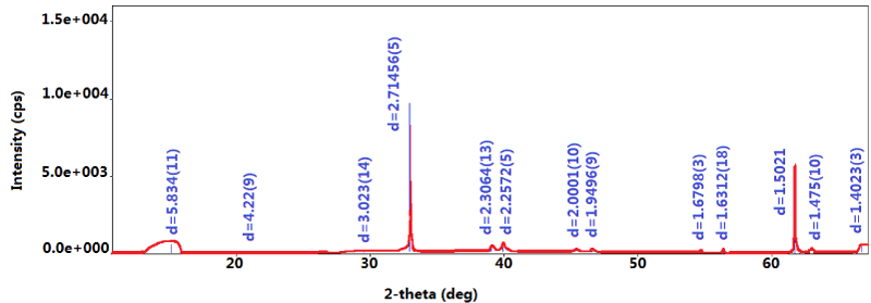
Figure 9.XRD of the hexagons
TEM and SAED patterns were also obtained from hexagons on TEM grids. Hexagons were transferred onto the TEM grids by scraping them from the substrates. Figure 10a shows the TEM image of one of the hexagon samples. The hexagons are crystalline, as is apparent from the diffraction patterns shown in the inset and in Figure 10. Some d-spacing values were measured and included on the SAED patterns. There exist many similarities to the values for type fibrous and violet phosphorus, however, there are also an equal number of spacing values that do not match up. Again, these d-spacing values were compared to the literature values and only partially matched with those of SnP.
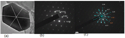
Figure 10. Transmission electron microscopy analysis of the hexagonal SnP structures. a) TEM image of a single hexagon, b, c) SAED analysis of the hexagon shown in a) showing the diffraction patterns.
Parallel lines were observed from the high resolution TEM image of the hexagons (Figure 11). The distance between two lines is 4.22 Å. It is well known that fibrous and violet phosphorus also show line patterns of the P8-P2-P9 cage tubes on high resolution TEM. However, the 4.22 Å d-spacing was not observed from the P8-P2-P9 cage tubes and the SnP single crystal [24]. Combining all the data observed, we hypothesize that the SnP hexagon has a different morphology from that of the SnP reported by Gullman [24]. It also contains tubes of cage clusters, although these tubes are most likely not be composed of P8-P2-P9 cages since the d-spacing numbers do not fully match with the ones for fibrous and violet phosphorus. Further experiments to achieve larger hexagons for single crystal analysis are necessary to fully characterize the molecular structure of the hexagons.
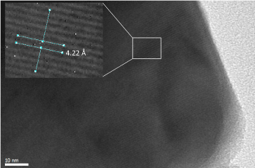
Figure 11. High resolution TEM image of a hexagon
By using a two-step method, fine hexagonal nanostructures of tin phosphide (SnP) were synthesized from the reaction of a RP film with Sn/SnI4 when the temperature and pressure are well controlled. The SnP hexagons seem to have a different morphology from that of the SnP reported. It also contains tubes of cage clusters, which are 4.22 Å apart. Some unique applications in electronic and optoelectronic fields of these hexagon are expected.
The authors would like to thank C. Johnson at the centralized Research Facility at Drexel University for his help with the TEM analysis.
- D. E. C. Corbridge, (2013) Phosphorus: Chemistry, Biochemistry and Technology, 6th ed, CRC Press.
- Bachhuber F, von Appen J, Dronskowski R, Schmidt P, Nilges T, et al. (2014) The extended stability range of phosphorus allotropes. Angew Chemie Int Ed 53: 1-6.
- Eckstein N, Hohmann A, Weihrich R, Nilges T, Schmidt P (2013) Synthesis and Phase Relations of Single-Phase Fibrous Phosphorus. Z Anorg Allg Chem 639: 2741-2743.
- Shirotani I (1982) Growth of large single crystals of black phosphorus at high pressures and temperatures, and its electrical properties. Mol Cryst Liq Cryst 86: 203-211.
- Endo S, Akahama Y, Terada S, Narita S (1982) Growth of large single crystals of black phosphorus under high pressure. Jpn J Appl Phys 21: L482-L484.
- Bridgman P (1914) Two new modifications of phosphorous. J Am Chem Soc 36: 1344-1363.
- Lange S, Schmidt P, Nilges T (2007) Au3SnP7@Black Phosphorus: An Easy Access to Black Phosphorus. Inorg Chem 46: 4028-4035.
- Köpf M, Eckstein N, Pfister D, Grotz C, Krüger I, et al. (2014) Access and in situ growth of phosphorene-precursor black phosphorus. J Cryst Growth 405: 6-10.
- Liu H, Neal AT, Zhu Z, Luo Z, Xu X, et al. (2014) Phosphorene: an unexplored 2D semiconductor with a high hole mobility. ACS Nano 4: 4033-4041.
- Wu J, Mao N, Xie L, Xu H, Zhang J (2015) Identifying the crystalline orientation of black phosphorus using angle-resolved polarized Raman spectroscopy. Angew Chemie Int Ed 54: 2366-2369.
- Smith JB, Hagaman D, Ji HF (2016) Growth of 2D black phosphorus film from chemical vapor deposition. Nanotech 27: 215602.
- Holleman AF, Wiberg E, Wiberg N (2007) Textbook of Inorganic Chemistry, (102nd edn), de Gruyter, Berlin, pp. 755-757.
- Liu Z, Huang X, Zhu Z, Dai J (2010) A simple mild hydrothermal route for the synthesis of nickel phosphide powders. Ceram Int 36: 1155-1158.
- Amaral PEM, Ji HF (2018) Stable Copper Phosphorus Iodide (Cu2P3I2) Nano/Microwire Photodetectors. ChemNanoMat 4: 1083-1087.
- Wolff A, Pallmann J, Boucher R, Weiz A, Brunner E, et al. (2016), Resource-Efficient High-Yield Ionothermal Synthesis of Microcrystalline Cu3-xP. Inorg Chem 55: 8844-8851.
- Wang K, Yang J, Xie J, Wang B, Wen Z (2003) Electrochemical reactions of lithium with CuP2 and Li1. 75Cu1. 25P2 synthesized by ballmilling. Electrochem Commun 5: 480-483.
- Pass G, Sutcliffe H (1974) Practical inorganic chemistry: preparations, reactions, and instrumental methods,(2nd edn), Chapman and Hall, pp: 9-10.
- Nilges T, Kersting M, Pfeifer T (2008) A fast low-pressure transport route to large black phosphorus single crystals. J Solid State Chem 181: 1707-1711.
- Roth WL, DeWitt TW, Smith AJ (1947) Polymorphism of Red Phosphorus. J Am Chem Soc 69: 2881-2885.
- Sugai S, Ueda T, Murase K (1981) Pressure Dependence of the Lattice Vibration in the Orthorhombic and Rhombohedral Structures of Black Phosphorus. J Phys Soc Japan 50: 3356-3361.
- Kaneta C, Katayama-Yoshida H, Morita A (1982) Lattice dynamics of black phosphorus. Solid State Commun 44: 613-617.
- a) Vanderborgh C, Schiferl D (1989) Raman studies of black phosphorus from 0.25 to 7.7 GPa at 15 K. Phys Rev B 40: 9595-9599; b) Sugai S (1984) Raman and infrared reflection spectroscopy in black phosphorus. Solid State Commun 53: 753-755; c) Akahama Y, Kobayashi M, Kawamura H (1997) Raman study of black phosphorus up to 13 GPa. Solid State Commun. 104: 311-315; d) Ribeiro HB, Pimenta MA, De Matos CJS, Moreira RL (2015) Unusual angular dependence of the Raman response in black phosphorus. ACS Nano 9: 4270-4276; e) Olego DJ, Baumann JA, Kuck MA, Schachter R, Michel CJ, et al. (1984) The microscopic structure of bulk amorphous red phosphorus: A Raman scattering investigation. Solid State Commun 52: 311-314.
- Ruck M, Hoppe D, Wahl B, Simon P, Wang Y, Seifert G (2005) Fibrous red phosphorus. Angew Chem Int Ed Engl 44: 7616-7619.
- Gullman J (1990) The crystal structure of SnP. J Solid State Chem 87: 202-207.