Abstract
For deposition of CdS thin films was successfully used a vacuum flash evaporation technique. XRD results have shown that all CdS films deposited at substrate temperatures of 100°C, 200°C and 300°C exhibit a predominant sharp peak at 2θ around 26.5° which can be assigned to the (002) plane of hexagonal structure. It was found that the intensity of diffraction peak (002) increases with a decrease of the substrate temperature. Average grain size calculated from XRD results is about 30 nm and weakly depends on the substrate temperature. It was found that after 30 min annealing at 400°C the intensity of (002) peaks increased considerably and at the same time average grain size growth only on 5-10%. Profiler results and AFM studies have shown that the roughness and morphology of the CdS thin film surfaces vary insignificantly with the variation of substrate and annealing temperature.
The transmission and reflection spectrum of CdS thin films measured in the spectral range 400–1000 nm. The optical bandgap is obtained by extrapolating the liner part of the plot of  vs. photon energy
  . The results of optical measurements have shown that the films deposited at substrate temperatures of 200°C and 300°C have optical bandgap 2.42eV which corresponds to the bandgap of bulk CdS crystal. After annealing the bandgap values were changed negligible.
Key words
cadmium sulfide (CdS), thin-film, solar cell, vacuum flash evaporation technique
Introduction
Cadmium sulfide (CdS) is a common material used in the formation of solar cells based on cadmium telluride (CdTe) and CuInGaSe2 (CIGS). In such solar devices n-type CdS thin-film acts as an optical window due to high bandgap energy Eg=2.42eV. For solar cells application CdS films have to have relatively high conductivity to reduce electrical loses of solar cells, thin thickness to provide high transmission and good uniformity in order to prevent electrical short-circuit effect. The structural, optical and electrical properties of CdS thin films strongly depend on the applied technique and the substrate temperature [1]. Different techniques have been reported for the deposition of CdS thin films namely: vacuum thermal evaporation [2-6], spray pyrolysis [7], electro-deposition [8] and chemical bath deposition [9-11]. Among other techniques the vacuum evaporation technique is very simple, inexpensive and is well established technique for the preparation of large area uniform films. In contrast to many other techniques the process of vacuum evaporation does not lead to heating the substrate, so allows to control the substrate temperature accurately by the external heating. Due to this feature vacuum evaporation technique is applicable for formation of solar cells on a flexible polyimide substrate. Replacing the glass substrate to a flexible substrate reduces the weight of thin film solar cells by 98%. Such solar cells are very promising for application on spacecraft so far as they have high ratio of electric power to weight. Flexible solar cells represent also of interest in the market for the terrestrial applications as they can easily be mounted on the surface of various shapes.
For fabrication of solar cell on flexible substrates it is necessary to use low-temperature film deposition techniques because polyimide substrates do not allow heating more than 450°C. As such techniques the most promising are the magnetron sputtering method and the method of vacuum thermal evaporation. For evaporation of multicomponent compound with different vapor pressure of components more suitable is the variant of vacuum thermal evaporation method notably the method of vacuum flash evaporation [12-17].
Distinguishing feature of this method is that the deposition of film is performed by continuous vacuum evaporation of small portions of multicomponent compound. Small particles of crushed multicomponent alloy whose constituents have different vapor pressure (for instance Cd and S in CdS) are falling into the preheated flash exchanger in a random way. Since the particles have different sizes and are falling in a random way in the flash exchanger at each moment there are some amount of particles which have different temperature and are at different evaporation stages of compound constituents. Simultaneous presence of such particles in the flash exchanger provides at the average the same fluxes of evaporated constituents and hence the stoichiometric composition of deposited film with pinpoints accuracy. Unfortunately as it is not surprising a very limited research works denoted to studies the characteristic of CdS films deposited by vacuum flash evaporation technique. This technique is also called a method of discrete evaporation.
The aim of this work was to study the structural, morphological and optical characteristics of nano-structured CdS thin films deposited on the glass substrates by flash evaporation technique as a transmittance and hetero layer in chalcogenide solar cells.
Experimental details
Thin films of CdS were fabricated by flash evaporation technique on commercial glass slides used as substrate with thickness 1 mm and diameter 20 mm. The substrates were thoroughly cleaned by soap-free detergent ultrasonically and then iteratively rinsing in distilled water to remove the traces of detergent. Thereafter the substrates were cleaned ultrasonically in ethanol and then dried by blowing air. The vacuum chamber before evaporation was pumped to a base pressure of 1.5×10⁻⁵ Torr.
Schematic view of flash evaporation setup is presented in (Figure. 1) The starting material was a pure bulk crystal of CdS which is crushed to a powder with particle dimensions of 50 μm –150 μm and then placed inside a batcher.
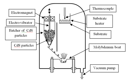
Figure 1. Schematic representation of the experimental setup.
Dispensing the CdS particles from batcher onto the molybdenum flash exchanger was performed due to opening and closing of batcher outlet by the instrumentality of electro-vibrator (Figure 1).
The amount of CdS particles falling into the flash exchanger was controlled by opening time of outlet. The outlet is opened when electro-vibrator attracts up by electromagnet. In our experiments the opening time was varied from 0.2 to 0.5 c. The outlet is opened again for evaporation of a next new portion of CdS particles only after evaporation of all particles contained in the flash exchanger. The evaporation process monitored through the chamber’s window.
Dispensing the CdS particles was started after the flash exchanger is heated up to temperature 1200°C - 1300°C suitable to evaporate the CdS powder. The distance between the flash exchanger and substrate was about 12 cm. The film thickness and the duration of deposition were typically 200-300 nm and 20-40 min. The CdS films were deposited at substrate temperatures of 100°C, 200°C and 300°C. As-deposited films were annealed at 400°C during 30 min in vacuum. The structural properties of samples were studied by X-ray diffractometer URD-6 in the q-2q mode using Cu - Ka (λ = 1.5405 Å) radiation. The surface morphology and roughness of CdS films were investigated by ZYGO profiler and by atomic force microscopy (AFM) type NEXT supplied by NT-MDT Inc. Transmittance and reflectance, over the wavelength from 400 to 1000 nm were measured using double beam Filmetrics F20 spectrophotometer.
Results and discussion
Structural properties of as-deposited and annealed CdS thin films
Figure 2 shows the X-ray diffraction patterns of as-deposited (red chart) and annealed (blue chart) CdS thin films deposited by flash evaporation technique on a glass substrate. Diffraction patterns were recorded over the 2θ range from 15° to 60° with the step 0.1°. XRD analyses showed that the CdS films were polycrystalline. Both as-deposited and annealed CdS films exhibit a predominant sharp peak at 2θ around 26.5° which can be assigned to either the (002) plane in the case of hexagonal structure [JCPDS card no: 41-1049] or the (111) plane in the case of cubic structure [JCPDS card no: 10-0454].
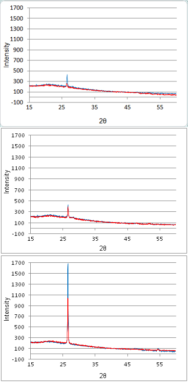
Figure 2. XRD patterns of CdS films as-deposited (red chart) at substrate temperature: a) 300°C, b) 200°C, c) 100°C and after annealed at 400°C during 30 min (blue chart)
The exact interpretation of XRD patterns it is quite difficult because most peaks of cubic and hexagonal CdS structure differ negligible within in the very small angle.
The summery of XRD data of as-deposited CdS thin films at different substrate temperature are presented in Table
1. In Table 2 are presented the summery of XRD data after annealing.
Table 1. XRD data of as-deposited CdS thin films at different substrate temperatures
Substrate
temperature |
2θ, (0) |
d (Å) observed from XRD |
d (Å) standard
JCPDS |
[hkl] plane |
c(Å) observed values |
c(Å) standard
JCPDS |
T=100°C |
26.518 |
3.3614 |
3.3567 |
002 |
6.7228 |
6.7134 |
T=200°C |
26.591 |
3.3523 |
3.3567 |
002 |
6.7046 |
6.7134 |
51.577 |
1.7721 |
1,761 |
112 |
x |
x |
T=300°C |
26.473 |
3.3670 |
3.3567 |
002 |
6.734 |
6.7134 |
51.546 |
1.7731 |
1,761 |
112 |
x |
x |
Table 2. XRD data of CdS thin films deposited at different substrate temperatures after annealing
Substrate
temperature |
2θ, (0) |
d (Å) observed from XRD |
d (Å) standard
JCPDS |
[hkl] plane |
c(Å) observed values |
c(Å) standard
JCPDS |
T=100°C |
26.541 |
3.3585 |
3.3567 |
002 |
6.7170 |
6.7134 |
T=200°C |
26.579 |
3.3537 |
3.3567 |
002 |
6.7074 |
6.7134 |
T=300°C |
26.524 |
3.3607 |
3.3567 |
002 |
6.7214 |
6.7134 |
It is seen from Table 1 that observed interplanar spacing-d and diffraction peaks in the XRD patterns when 2θ = 26.518° (substrate temperature 100°C), 2θ =26.591°, 2θ =51.577° (substrate temperature 200°C), 2θ = 26.473°, 2θ =51.546° (substrate temperature 300°C) correspond with reflection from the crystal planes (002), (112) of CdS hexagonal structure, which agrees well with standard XRD patterns (JCPDS card no: 41-1049). The same results of hexagonal structure are observed for CdS thin films deposited by flash evaporation technique in work [14].
After annealing, as can be seen from Table 2 the structure of the deposited films clearly changed. After annealing the peaks around 2θ = 51° (for CdS films as-deposited at 200°C and 300°C) disappeared and the predominant sharp peaks at 2θ around 26.5° drastically have increased (Figure 2, blue charts).
The structural parameters of as-deposited and annealed CdS thin films such as the average grain sizes (D), dislocation density (δ), the number of crystallites per unit area (N) and micro-strain (ε) for comparison are presented in Table 3.
Table 3. Structural parameters of CdS films as-deposited at substrate temperature 100°C, 200°C and 300°C and after annealing at 400°C during 30 min
Substrate
temperature |
2θ, (0) |
FWHM
(deg)
|
D (nm) from XRD results |
[hkl] plane |
δ
1015
lines/m2 |
ε
x10-4 |
N
x1015 m-2 |
Thickness of films (nm) (t) |
|
as-depo-sited |
annealed |
as-depo-sited/
annealed |
as-depo-sited |
annea-led |
as-depo-sited/
annea-led |
as-depo-sited |
annea-led |
as-depo-sited |
annea-led |
as-depo-sited |
annea-led |
as-depo-sited/
annea-led |
T=100°C |
26.518 |
26.541 |
0.35/0.3 |
29.49 |
34.74 |
002 |
1.15 |
0.83 |
11.8 |
10 |
8.576 |
5.246 |
220 |
T=200°C |
26.591 |
26.579 |
0.35/0.35 |
30.43 |
30.27 |
002 |
1.08 |
1.09 |
11.4 |
11.5 |
8.514 |
8.650 |
240 |
T=300°C |
26.473 |
26.524 |
0.35/0.35 |
28.96 |
29.57 |
002 |
1.2 |
1.14 |
12 |
11.7 |
12.353 |
11.6 |
300 |
The average grain sizes (D) of the film was calculated using the Scherrer’s equation [18]:
where λ is the wavelength of the X-ray used (λ=1.5405 Å),  β is the full-width at half-maximum (FWHM) of the (002) peak which has maximum intensity, and
(Θ)
is the Bragg’s angle.
β is the full-width at half-maximum (FWHM) of the (002) peak which has maximum intensity, and
(Θ)
is the Bragg’s angle.
The variation of the grain size with substrate temperature is presented in Table 3. It is seen that the grain size vary insignificantly. The biggest grain size (30.43 nm) observed for CdS film as-deposited at 200°C and (34.74 nm) for CdS film deposited at 100°C after annealing.
The dislocation density δ defined as the length of dislocation lines per unit volume, has been calculated using the equation [19]: δ=1/D2. The results of calculation are presented in Table 3. The small values of (δ) confirmed the good crystallinity of the CdS films. The number of crystallites per unit area (N) and the micro-strain (ε) of the films have been estimated with the use of the following equations [20]: N=t/D3 and ε=β cos(θ)/4. It is seen from Table 3 the annealing led to decreasing the micro-strains and number of crystallites per unit area of all as-deposited films. The lower values of micro-strains and the number of crystallites per unit area observed for as-deposited CdS films at 200°C and for CdS film deposited at 100°C after annealing.
Optical properties of as-deposited and annealed CdS thin films
Using transmittance (T) and reflectance (R) spectra the absorption coefficient has been calculated by the following equation:
where t is the thickness of CdS film.
Above the fundamental absorption edge the dependence of the absorption coefficient on the incident photon energy is given by Tauc’s model [21]:
where  is the photon energy, Eg is the optical bandgap, B is a constant and n is an exponent that depends on the type of optical transitions. For direct allowed transitions n=½. The variation of
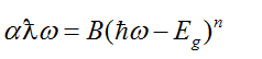
  of CdS thin films deposited at different substrate temperatures as a function of photon energy are shown in Figure 3. In Figure 4 are presented the variation of vs. photon energy of CdS thin films after annealing.
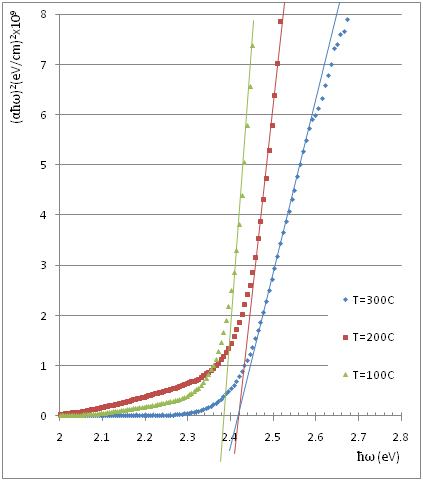
Figure 3. Plots of (2 vs. photon energy  of CdS thin films deposited at 100°C, 200°C and 300°C substrate temperatures.

 Using the liner extrapolation method the value of the optical bandgap for as-deposited CdS thin films is determined to be 2.39, 2.42 and 2.42 eV for 100°C, 200°C and 300°C, accordingly. After annealing the optical bandgap is changed insignificantly and became 2.38, 2.40 and 2.40 eV, accordingly. The results of measurements have shown that the CdS thin film deposited at 200°C and 300°C have the same optical bandgap as the bulk of CdS crystal Eg = 2.42 eV.
Morphological properties of as-deposited and annealed CdS thin films.
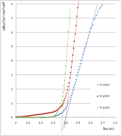
(Figure 5) shows typical 1,5 μm × 1,5 μm AFM images of CdS films deposited on a glass substrate at different temperatures by flash evaporation technique. For statistics a few AFM images of different sites of the surface of each sample were investigated. Profiler results and AFM images show that the morphology and roughness of the surface weakly depends on the substrate temperature. A typical AFM images for as-deposited and annealed CdS thin films are presented in Figure 5 and Figure 6 respectively.
2021 Copyright OAT. All rights reserv
Figure 4. Plots of 2 vs. photon energy of CdS thin films deposited at 100°C, 200°C and 300°C substrate temperatures after annealing at 400°C during 30 min in vacuum
Figure 5. A typical AFM images and the distribution of grain size of as-deposited CdS thin films on a glass substrate at 100°C.
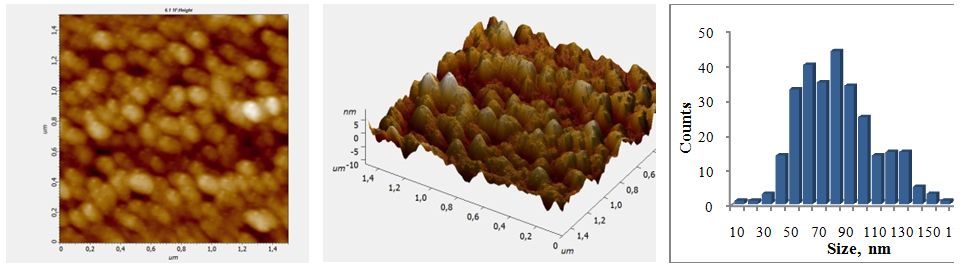
Figure 6. A typical AFM images and the distribution of grain size of CdS thin films deposited on a glass substrate at 100°C after annealing
Conclusion
The structural, morphological and optical properties of the CdS thin films deposited on glass substrate at different temperatures (100°C, 200°C and 300°C) by vacuum flash evaporation technique have been investigated. The annealing effect on these properties has also been investigated. XRD results showed that both all of as-deposited at different temperatures and annealed CdS thin films were polycrystalline, have hexagonal structure and exhibit a predominant sharp (002) peak at 2θ around 26.5°. It is found that the intensity of diffraction peak (002) increases with a decrease of the substrate temperature. After annealing the peak at 2θ = 51° (for CdS films as-deposited at 200°C and 300°C) disappeared and the predominant sharp peaks at 2θ = 26.5° increased.
Using XRD results the structural parameters of CdS thin films such as the average grain sizes (D), dislocation density (δ), the number of crystallites per unit area (N) and micro-strain (ε) was calculated. These results have shown that the best crystalline structure have CdS films as-deposited at 200°C and CdS films deposited at 100°C after annealing.
The results of optical measurements have shown that CdS thin films deposited at 100°C have 2.39eV bangap and 2.42eV bandgap have films deposited at 200°C and 300°C. This value of bandgap (2.42eV) is equal to the bandgap of CdS bulk crystal. These values of bandgap after annealing slightly decreased from 2.39eV to 2.38eV and from 2.42eV to 2.40eV.
As showed the AFM images and profiler measurements the roughness of the CdS films is 5-8nm and weakly depends on both substrate temperature and annealing.
References
- 1. Hewig GH, Bloss WH (1977) Technology of thin film solar cells. Thin Solid Films 45: 1-7.
- 2. Senthil K, Mangalaraj D, Narayandass SK, Adachi S (2000) Optical constants of vacuum-evaporated cadmium sulphide thin films measured by spectroscopic ellipsometry. Materials Science and Engineering: B, 78: 53-58.
- 3. Iacomi F, Purica M, Budianu E, Prepelita P, Macovei D (2007) Structural studies on some doped CdS thin films deposited by thermal evaporation. Thin Solid Films 372: 6080.
- Sathyamoorthy R, Chandramohan S, Sudhagar P, Kanjilal D, Asokan K (2006) Structural and photoluminescence properties of swift heavy ion irradiated CdS thin films. Sol Energy Mater &Sol Cells 90: 2297.
- 4. Mahmoud SA, Ibrahim AA, Riad AS (2000) Physical properties of thermal coating CdS thin films using a modified evaporation source.Thin Solid Films 372: 144.
- 5. Ashour A, El-Kadry N, Mahmoud SA (1995) on the electrical and optical properties of CdS films thermally deposited by a modified source.Thin Solid Films 269: 117.
- 6. Baykul MC, Balcioglu A (2000) AFM and SEM studies of CdS thin films produced by an ultrasonic spray pyrolysis method. Microelectronic Engineering 51: 703-713.
- 7. Nishino J, Chatani S, Uotani Y, Nosaka Y (1999) Electrodeposition method for controlled formation of CdS films from aqueous solutions. Journal of Electroanalytical Chemistry 473: 217-222.
- 8. Moualkva H, Hariech S, Aida MS (2009) Structural and optical properties of CdS thin films grown by chemical bath deposition, Thin Solid Films 518:1259–62.
- 10. Pushpalatha HL, Ganesha R (2014) Structural and morphological studies of CdS thin films grown by photochemical deposition. International Journal of ChemTech Research 6: 1998-2001
- 11. Khallaf H, Oladeji IO, Chai G, Chow L (2008) Characterization of CdS thin films grown by chemical bath deposition using four different cadmium sources. Thin Solid Films 516: 7306-7312.
- 12. Gevorkyan VA, Reymers A E, Nersesyan M N, Arzakantsyan M (2012) Characterization of Cu2O thin films prepared by evaporation of CuO powder. In Journal of Physics: Conference Series IOP Publishing.
- 13. Hemanadhan M, Bapanayya C, Agarwal SC (2010). Simple flash evaporator for making thin films of compounds. Journal of Vacuum Science & Technology 28: 625-626.
- 14. Ehsani M H, Dizaji HR (2011) A modified feeder in flash evaporation technique and fabrication of CdS thin films. Chalcogenide Letter 8
- 15. Hasoon SA, Ibrahim I M, Al-Haddad RM, Mahmood SS (2014) Fabrication of nanostructure CdS thin film on nanocrystalline porous silicon. Int J Curr Eng Technol 4: 594-601
- 16. Murali KR, Kannan C, Subramanian K (2008) Photo-electrochemical properties of flash evaporated cadmium sulphide films.Chalcogenide letters 5: 195-199.
- 17. Shah NM, Ray JR, Kheraj VA, Desai MS, Panchai CJ (2009) Structural, optical, and electrical properties of flash-evaporated copper indium diselenide thin films J Mater Sci 44: 316-322.
- 18. Cullity BD (1957). Elements of X-ray Diffraction. American Journal of Physics 25: 394-395
- 19. Bilgin V, Kose S, Atay F, Akyuz I (2005) The effect of substrate temperature on the structural and some physical properties of ultrasonically sprayed CdS films. Materials Chemistry and Physics 94: 103-108.
- 20. Dhanam M, Prabhu RR, Manoj PK (2008) Investigations on chemical bath deposited cadmium selenide thin films. Materials Chemistry and Physics, 107: 289-296.
- 21. Tauc J, Grigorovici R, Vancu A (1966). Optical properties and electronic structure of amorphous germanium. Physica Status Solidi 15: 627-637.