Abstract
Graphene/Bi2Se3/Graphene (G/Bi2Se3/G) sandwich hybrids were fabricated via chemical vapor deposition. The medium graphene layer is used to synthesize the high-quality Bi2Se3, benefitting from the smaller lattice mismatch between graphene and Bi2Se3. The covering graphene layer is designed to inhibit the surface oxidation of Bi2Se3 layers which are easily changed to BiOx in the atmosphere. The Raman spectroscopy, scanning electron microscopy and X-ray diffraction confirm the high-quality and uniform Bi2Se3 film. The Raman spectroscopy and X-ray diffraction investigates antioxidant ability of the G/Bi2Se3/G structure. We conclude that the graphene can effectively improve the crystal quality of Bi2Se3 and inhibit the surface oxidation of it.
Graphical abstract
The method to improve the crystal quality and inhibit the surface oxidation is important for the application of the Bi2Se3 films. Graphene/Bi2Se3/Graphene (G/Bi2Se3/G) sandwich hybrids were fabricated here via chemical vapor deposition. The medium graphene layer is used to synthesize the high-quality Bi2Se3, benefitting from the smaller lattice mismatch between graphene and Bi2Se3. The covering graphene layer is designed to inhibit the surface oxidation of Bi2Se3 layers which are easily changed to BiOx in the atmosphere. We conclude that the graphene can effectively improve the crystal quality of Bi2Se3 and inhibit the surface oxidation of it.
Key words
sandwich hybrid, Bi2Se3 film, surface oxidation
Introduction
Bi2Se3, an ideal topological insulator (TI) with a single Dirac cone residing in a large bulk bandgap (~0.3ev), has attracted extensive scientific interests to experimental and theoretical communities [1]. Layer-structured Bi2Se3 materials may be applied for the future spintronics and quantum computing devices due to large ratio of surface-to-volume, thus it is urgent to synthesize high-quality Bi2Se3 with defined sizes [2-4]. Various methods have been tried to fabricate Bi2Se3 thin film, such as molecular beam epitaxial (MBE) [5,6], solvothermal synthesis [7], mechanical exfoliation [8], metal-organic chemical vapor deposition (MOCVD) [9] and chemical vapor deposition (CVD) [10-13]. Compared with other methods, CVD is an inexpensive and effective strategy to obtain Bi2Se3 materials. Directly fabricated the large-area high-quality Bi2Se3 film on SiO2 is difficult due to the larger lattice mismatch between Bi2Se3 and SiO2. Graphene film, a 2-D atomic-scale honeycomb lattice made of carbon atoms, can be used to fabricate the high-quality epitaxial layer benefiting from that the van der Waals interactions between epitaxial layer and graphene can efficiently suppress the negative effects of the lattice mismatch [12]. Here, we fabricated large-area high-quality Bi2Se3 thin film in a Se-rich environment via a catalyst-free CVD method on the graphene/SiO2 substrate.
However, the synthesized Bi2Se3 thin film gets doped after being exposed to the atmosphere and the content of BiOx increased with the increase of the exposed time. Such rapid surface oxidation reduces the relative contribution of surface states, which greatly limits the development of the Bi2Se3 devices [14]. Therefore, a method to inhibit the surface oxidation is urgently required. Graphene is capable of both scavenging free-radicals [15–18] and can serving as gas barriers [19–23], these dual effects make graphene be effective in improving oxidation stability of Bi2Se3. In this study, we fabricated high-quality G-Bi2Se3-G heterostructure via CVD. There are two advantages of this heterostructure: (1) the 2D growth single-crystal Bi2Se3 thin film can be successfully deposited on the graphene film; (2) the oxidation process of the Bi2Se3 is significantly delayed compared with that without the protection of the graphene.
Experimental method
The monolayer graphene film was synthesized on the Cu foil via a CVD method and immediately transferred to the SiO2 substrate using wet-etching process. Bi2Se3 thin film was grown on the monolayer graphene substrate along the lateral direction with the help of Se powder in the source materials via CVD method in a horizontal quartz tube (~3.5 inch in diameter), which has been investigated by our previous work [13]. As shown in Figure 1, high purity powder of Bi2Se3 and Se as the precursor for evaporation was located in the constant-temperature zone and the G/SiO2 substrate was placed on a quartz boat in the down-stream zone. The horizontal quartz tube was pumped to 1.0×10⁻⁶ Torr by mechanical pump and aerated Ar gas with ~50 sccm flow rate to remove any oxygen residue. The constant- temperature zone of the furnace was heated and maintained at 550°C for 15 min. The furnace was naturally cooled down to the ambient temperature with the Ar gas flowing (~50 sccm). The fabricated Bi2Se3/G is immediately covered by another graphene layer to get the G/Bi2Se3/G sandwich hybrid structure. Following the fabrication, the morphology, chemical analysis, structural properties and single-crystalline structure of the G/Bi2Se3/G were characterized by scanning electron microscopy (SEM), energy dispersive X-ray spectroscopy (EDS), Raman spectroscopy and X-ray diffraction (XRD).
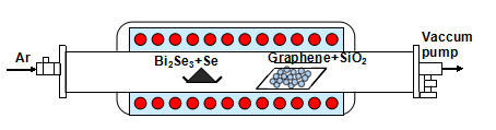
Figure 1. Schematic of the hot-wall CVD system used in this study.
Results and discussion
Graphene layer plays a vital role in forming uniform Bi2Se3 thin film. Figure 2. (a) exhibits the SEM image of the Bi2Se3 deposited on the SiO2 substrates with and without the graphene film. From the right of the Figure 2(a), only Bi2Se3 nanoplates were obtained in the case of no graphene serving as medium layer, which can be easily observed from SEM image under a high magnification (shown in the Figure 2(b)). As can be seen, the Bi2Se3 nanoplates grow along the lateral direction with the help of the Se powder in the source materials serving as growing point. However, the large lattice mismatch with SiO2 substrates makes it impossible to form Bi2Se3 film. Large area high-quality Bi2Se3 thin film was synthesized on the graphene/SiO2 on the left of the images, which benefits from the van der Waals interactions between the graphene and Bi2Se3 layer. Figure .2(c) shows the SEM images of Bi2Se3 samples grown on SiO2 substrate with the graphene layer under 10× magnificant, symmetric triangular and hexagonal morphologies with a smooth multi-layered structure aligned in the same orientation. Individual Bi2Se3 plates deviated from the main orientation may be introduced by the lattice mismatch or defects of the graphene substrate. The EDX spectrum of the samples displayed in Figure . 2(d) shows that the energy signal peak of Se and Bi are detected on the G/SiO2 substrate. Table 1 provides that atomic ratio of Se and Bi is nearly equal to the stoichiometric ratio of 1.5 for Bi2Se3, concluding that we have produced Bi2Se3 thin film with uniform chemical composition.
Table 1. Quantitative atomic analysis of the Bi and Se elements.
|
Element
|
Weight%
|
Atomic%
|
|
C
|
0.39
|
2.68
|
|
O 10.53
|
10.53
|
34.02
|
|
Si
|
20.78
|
38.24
|
|
Se
|
22.52
|
14.7 4
|
|
Bi
|
45.77
|
10.3 2
|
|
Totals
|
100.0
|
|
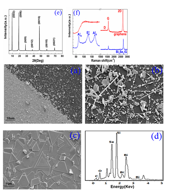
Figure 2. (a) The SEM image of the Bi2Se3 deposited on the SiO2 substrates with and without the graphene film. (b) High magnification SEM image of Bi2Se3 nanoplates grown on the SiO2 substrate. (c) High magnification SEM image of the Bi2Se3 thin film deposited on the G/SiO2 substrate. (d) EDX spectrum of the Bi2Se3/G hybrid materials. (e) 2θ–ω X-ray diffraction pattern of the prepared sample. (f) The Raman spectra of the graphene and Bi2Se3/G.
It is possible to verify the crystal structure of the Bi2Se3 thin film by XRD measurement. As shown in Figure 2(e), only (003) family peak including (003), (006), (009), (0012), (0015), (0018) and (0021) are detected, proving that the sample has a good c-axis orientation and periodic. FWHM of lattice diffraction peaks is less than 0.03 [24], indicating a high quality of the Bi2Se3 single crystal.
In order to give a more definite identification of crystal quality of Bi2Se3 single crystal,Raman spectroscopy were carried out at room temperature. The typical Raman spectra of the graphene and Bi2Se3/G on the SiO2 substrate are simultaneously shown in Figure 2(f). In the low frequency region, the spectrum of the graphene is rising, which may be related with the SiO2 substrates. The spectrum of the Bi2Se3 reveals three characteristic bands of the Bi2Se3 thin film: ~72, ~131 and ~174 cm−1 respectively correspond to the

 and vibrational modes [25]. The symmetric Lorentzian line shape of all of the Raman peaks means that the Bi2Se3 thin film samples have a crystal structure. Obvious G and 2D bands at ~1585 and ~2700 cm-1 representing for graphene film, were also detected in the high frequency region. The intensity ratio of the 2D peak to G peak was measured to be around 2.0, which are typical signatures of a monolayer graphene film. In addition, after the deposition of the Bi2Se3 thin film, the 2D band of the monolayer graphene film becomes broader and up shifts by ~28 cm-1, which probably be attributed to the van der Waals interaction of the Bi2Se3 thin film and graphene. These features imply the fact that the graphene film still possesses perfect structural properties after the deposition of the Bi2Se3 thin film.
Quintuple layer (QL) in Bi2Se3 is ordered in a Se–Bi–Se–Bi–Se sequence via covalent bond and adjacent layer are connected by weak van der Waals force. Dangling bonds appeared in the surface of Bi2Se3 film as a result of the Se vacancies make Bi2Se3 easily react with oxygen atoms of environment and form BiOx [11,14], which great limit the application of Bi2Se3. The stability of the Bi2Se3 sample as a function of exposure time in air as shown in Figure 3(a), the Raman modes at 72 cm−1, 131cm−1, 174 cm−1 attributed to Bi2Se3 are clearly seen. However, the modes of BiOx at 250 cm−1 and 328 cm−1 [26] appears when the sample is left in air over ten days. To further demonstrate the formation of BiOx, XRD measurement was carried out as shown in Figure 3(b), the diffraction peaks of BiOx at 2θ= 27.377, 40.053 and 41.884 appears respectively [11], which correspond well with the Raman spectrum (shown in Figure 3(a). It illustrates that the formation of BiOx is very fast.
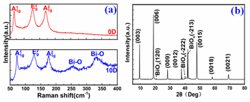
Figure 3. (a) The Raman spectrum of the Bi2Se3/G sample respectively exposed in air for 0 day and 10 days. (b)
2θ–ω X-ray diffraction pattern of the Bi2Se3/G sample exposed in air.
In order to delay the oxidation of Bi2Se3 film, we transfer a covering
graphene on it again to fabricate a G/Bi2Se3/G sandwich Dirac heterostructure. The covering graphene can be mixed with Bi2Se3 thin film at a molecular level to maximize the contact between them by the van der Waals interaction [22]. The monolayer graphene are stable under ambient conditions and its pore size is far less than the size of oxygen molecules, which make it a perfect gas barrier. In addition, it is capable of scavenging free-radicals, thus the covering graphene layer can effectively delay the process of surface oxidation of Bi2Se3 [23]. The Raman spectrum signal of the G/Bi2Se3/G sample shown in Figure 4(a) is different from the Raman spectra changes of the Bi2Se3/G sample and remains unchanged continuously. It provides us a definite experimental evidence that the covering graphene can effectively delay the surface oxidation of Bi2Se3.
2021 Copyright OAT. All rights reserv
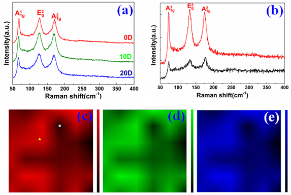
Figure 4. (a) The Raman spectrum of the G/Bi2Se3/G sample exposed in air for different days. (b) Raman spectrum respectively from the point marked in (c) by the yellow triangle (red) and white dot (black). (c)-(e) The scanning Raman , band mappings of the G/Bi2Se3/G sample, respectively.
We carried out a 10 ×10 μm2 Raman
,
and band mappings of the G/Bi2Se3/G sample to prove the chemical stability of it. As we all known, the intensity of the out-of-plane vibrational mode,
and
peak, is more sensitive to the thickness [25]. The thickness of the G/Bi2Se3/G films can be identified by the Raman band mappings with the different color. As can be seen from Figure 4(c), (d) and (e), relatively smooth
, and
, band mappings of Bi2Se3 thin film with uniform colour are formed, indicating the large-area layer-controlled Bi2Se3 thin film. In Figure 4(b), the red spectrum is taken from the red region marked by the yellow triangle in Figure 4(c). It presents the typical characteristics of the smooth Bi2Se3 film: obvious bands
,
and
,
at ~72, ~131 and ~174 cm-1. As can be seen, the intensity of
,
and
,
peak is lower than that of
peak (in-plane mode), which is the representative of high quality and uniform Bi2Se3 thin film with stable chemical properties. The black region of the band mapping is formed due to the different thickness of the prepared Bi2Se3 thin film, which still features a micro-scale inhomogeneity structure. The black spectrum in Figure 4(b) is obtained from the black region in Figure 4(c), which is marked by the white dot. The intensity of
,
and
,
is stronger than that of
, describing the thicker layer of Bi2Se3 are formed, well corresponding with the band mapping of the sample. The mode of BiOx (250 cm−1 and 328 cm−1) can’t be obtained consistently, concluding that the covering graphene layer is an effective packaging material to inhibit the oxidization process of Bi2Se3 under ambient conditions.
Conclusion
In conclusion, we have demonstrated that high-quality and uniform Bi2Se3 thin film can be obtained with graphene serving as medium layers and the covering graphene can effectively delay the process of surface oxidation of Bi2Se3. This method presents a simple and economical technique to fabricate Bi2Se3 film with chemistry stable under ambient conditions. It presents a practical help for probing topological insulator surface state by transport measurements and pave the way for applying in the spintronics and quantum computing.
Acknowledgments
The authors are grateful for financial support from the National Natural Science Foundation of China (11474187, 11274204, 61205174).
References
- Cui HM, Liu H, Wang JY, Li X, Han F, Boughton RI (2004) Sonochemical synthesis of bismuth selenide nanobelts at room temperature. J Cryst Growth 271: 456-461.
- Peng HL,Lai KJ,Kong DS,Meister S,Chen YL, et al. (2010) Aharonov-Bohm interference in topological insulator nanoribbons. Nat Mater 9: 225-229. [Crossref]
- Tang H,Liang D,Qiu RLJ, Gao XPA (2011) Two-dimensional transport-induced linear magneto-resistance in topological insulator Bi2Se3 nanoribbons. ACS Nano 5: 7510-7516. [Crossref]
- Xiu FX, He L,Wang Y,Cheng YL, Chang LT, Lang MR , et al. (2011) Manipulating surface states in topological insulator nanoribbons. Nanotech 6: 216-22. [Crossref]
- He L, Xiu FX, Wang Y, Alexei V, Fedorov G, et al. (2011) Epitaxial growth of Bi2Se3 topological insulator thin films on Si. J Appl Phys 109: 103702
- Tabor P, Keenan C, Urazhdin S, Lederman D (2010) Plasmon-enhanced electron-phonon coupling in Dirac surface states of the thin-film topological insulator Bi2Se3. Nature Physics 6: 584-588.
- Zhang GQ, Wang W, Lu XL, (2009) Solvothermal Synthesis of V− VI Binary and Ternary Hexagonal Platelets: The Oriented Attachment Mechanism. Growth Des 9: 145-150.
- Checkelsky JG, Hor YS, Liu MX, Qu DX, Cava RJ, Ong NP (2009) Quantum interference in macroscopic crystals of nonmetallic Bi 2 Se 3. Phys Re Lett 103: 246601. [Crossref]
- Alegria LD, Schroer MD, Chatterjee A, Poirier GR, Pretko M, et al. (2012) Structural and Electrical Characterization of Bi2Se3 Nanostructures Grown by Metal-Organic Chemical Vapor Deposition. Nano Lettr 12: 4711-4714. [Crossref]
- Dang WH, Peng HL, Li HL, Wang P, Liu ZF (2010) Epitaxial heterostructures of ultrathin topological insulator nanoplate and graphene. Nano Lett 10: 2870 -2876. [Crossref]
- Liu FY, Liu M, Liu AH, Yang C, Chen CS, et al. (2015). J Mater Sci 26: 3881-3886
- Zhang C, Liu M, Man BY, Jiang SZ, Yang C, Chen CS, et al. (2014) Cryst Eng Comm16: 8941
- Liu M, Liu FY, Man BY, Bi D, Xu XY (2014) Multi-layered nanostructure Bi 2 Se 3 grown by chemical vapor deposition in selenium-rich atmosphere. Appl Surf Sci 317: 257-261
- Kong DS , Cha JJ, Lai KJ, Peng HL, Analytis JG , Meister S, et al. (2011) Evaporative Thinning: A facile synthesis method for high quality ultrathin layers of 2D crystals. Am Chem Soc 5: 4698-4703.[Crossref]
- Qiu Y, Wang Z, Owens AC, Kulaots I, Chen Y, et al. (2014) Antioxidant chemistry of graphene-based materials and its role in oxidation protection technology. Nanoscale 6: 11744-11755. [Crossref]
- Denis PA, Iribarne F (2012) A First‐Principles Study on the Interaction between Alkyl Radicals and Graphene. Chem Eur J 18: 7568-7574. [Crossref]
- Wang FT, Chen L, Tian CJ, Meng Y, Wang ZG, et al. (2011) Interactions between free radicals and a graphene fragment: Physical versus chemical bonding, charge transfer, and deformation. J Comput Chem 32: 3264-3268. [Crossref]
- Yang Y, Huang Y, Lv Y, Zhao P, Yang Q, et al. (2013) Mater Chem A1: 11184-11191.
- Kim H, Miura Y, Macosko CW (2010) Graphene/polyurethane nanocomposites for improved gas barrier and electrical conductivity.Chem. Mater 22: 3441-3450.
- Wu JR, Huang GS, Li HL, Wu, SD, Liu YF, et al. (2013) Enhanced mechanical and gas barrier properties of rubber nanocomposites with surface functionalized graphene oxide at low content. Polymer 54: 1930-1937.
- Potts JR, Shankar O, Du L, Ruoff RS (2012) Processing-morphology-property relationships and composite theory analysis of reduced graphene oxide/natural rubber nanocomposites. Macromolecules 45: 6045-6055.
- Tang MZ, Xing W, Wu JR, Huang GS, Xiang KW, et al. (2015) Graphene as a prominent antioxidant for diolefin elastomers. J Mater Chem A 3: 5942.
- Chen ZS, Biscarasa J, Shukla A (2015) A high performance graphene/few-layer InSe photo-detector. Nanoscale 7: 5981. [Crossref]
- Zhang M, Yang LQ, Yang XS , Zhao Y (2013) Materials Review 27: 7.
- Zhang J, Peng ZP, Soni A, Zhao Y, Xiong Y, et al. (2011) Raman spectroscopy of few-quintuple layer topological insulator Bi2Se3 nanoplatelets. Nano Lett 11: 2407-2414. [Crossref]
- Salazar-Pérez AJ, Camacho-López MA, Morales-Luckie RA, Sánchez-Mendieta V (2005) Structural evolution of Bi2O3 prepared by thermal oxidation of bismuth nano-particles.Superficies y Vacio18: 4-8.