Novel nanostructured island sites are made to decorate a microporous/nanoporous array. These island sites are formed from a variety of easily produced nanostructured metal oxides deposited from solution. Sensor platforms are distinct from and do not require film-based coating. The nanostructure directing acidic metal oxide sites which vary in their Lewis acidity decorate micropores and control the electron transduction process. The interaction of analytes with these island sites varies in a predictable manner and can be modified through in-situ functionalization of their Lewis acidity. The microporous structure allows rapid Fickian diffusion of analytes to the active nanostructure island sites whose reversible interaction dominates the sensor response as it requires low energy consumption. Highly accurate repeat depositions are not required. We require that the island sites are deposited at sufficiently low concentration so as not to interact electronically with each other. The response time of these interfaces is more rapid than film-based depositions, which require a more lengthy diffusion time. The sensors are reversible. The nanoporous structure prevents sintering of these island centers at elevated temperatures. The concentration of detection centers can be made to produce an optimum matrix of enhanced sensor responses, force a dominant distinct analyte-interface physisorption (rather than chemisorption). The produced semiconductor interface is easily functionalized to create an enhanced range of nanoparticle semiconductor sites. The matrix provides a sensitive means of transferring electrons that are easily detected. The sensors operate at room temperature as well as elevated temperatures. Low energy magnetic field signal enhancement can be achieved with transition metals. Contaminated sensors can be readily rejuvenated. Pulsed mode operation ensures low analyte consumption and high analyte selectivity and further provides the ability to rapidly assess false positive signals using Fast Fourier Transfer techniques, Solar pumped sensors requiring low light levels (≤ 1 Watt) have been demonstrated. Water vapor contamination can be greatly if not entirely reduced. The modelling of sensor response with a new Fermi energy distribution –based response isotherm is found to be superior to other isotherms. Sensors operate can be made to operate efficiently for two gases simultaneously. Modes of extending these studies to multiple gas arrays are considered.
We have used a variety of etch procedures to produce a range of resultant pore morphologies which suggest several applications of porous silicon (PS) interfaces combining micro- and nanopore technology [1,2]. Select micro/nanoporous interfaces have been formed and treated to provide an active scaffolding, extending efficient sensor configurations to efficient photocatalytic microreactors that can be actively microfiltered to provide PS-based lithium microbattery configurations [3,4]. To provide sensor configurations that operate sensitively, selectively, rapidly, and reversibly at room temperature a range of nanoparticle modified microporous arrays have been developed. This article will focus primarily on these sensor systems.
A New Sensor Interface and Novel Sensor Attributes
We have developed a novel approach to chemical sensor technology, which can lead to significant improvements in the operation of gas sensors and sensor arrays. Interfaces formulated with a novel, rational, and inexpensively implemented concept are tailored to target specifications, operative across wide temperature and pressure ranges [5]. They have the potential, as well, for extension to mixed analyte environments [6]. Our patened etch process coupled with nanoparticle providing solutions creates a nanoparticle covered microporous array to form distinct electronically independent detection centers. The nanoporous structure prevents sintering of these island centers at elevated temperatures. The concentration of detection centers can be made to produce an optimum matrix of enhanced sensor responses vastly superior to that based on surface coating techniques. The nanostructure island sites, within the micropores, force a dominant distinct analyte-interface physisorption (rather than chemisorption), The metal oxide decorated semiconductor interface can be easily functionalized to create an enhanced range of nanoparticle semiconductor sites as the matrix provides a sensitive means of transferring electrons that are easily detected [7].
The Sensor Attributes may be summarized as follows
The sensors are simple in design, operate in a saturated or unsaturated mode, and demonstrate considerably higher sensitivities than traditional metal oxide sensors. Simple sensor platforms do not require a film coated micro-porous array, are deposited with nanostructure directing acidic metal oxide sites which vary in their Lewis acidity, decorate micropores and control the electron transduction process. The interaction of analytes with these island sites varies in a predictable manner and can be modified through in-situ functionalization of their Lewis acidity. The microporous structure allows rapid Fickian diffusion of analytes to the active nanostructure island sites whose reversible interaction with the analyte dominates the sensor response. Highly accurate repeat depositions is not required. We require only that the island sites be deposited at sufficiently low concentration so as not to interact electronically with each other. The nanoparticle island sites are selected for deposition from a variety of easily obtained solution-based sources as the forgiving deposition process requires a minimum of energy consumption and time [5,7].
The sensors are operative at room temperature as well as elevated temperatures with an insensitivity to temperature drift. When heat-sunk, the configuration allows reliable performance at a surface temperature ~ 100°C even in elevated temperature environments (e.g. combustion or flue gas) in sharp contrast to typical metal oxide sensors [8]. The sensors have a rapid response, high sensitivity (near ppb), and reversibility [7]. The ease of modification with a diversity of clearly mapped and readily generated gas-selective nanostructured materials provides a range of sensitivities for a broad range of gases as well as being formatable for sensor arrays (response matrix) [5].
The sensors are energy- efficient with low power requirements (microwatts-less than a watch battery), and sensitivity, as weak physisorptive processes produce a conductometric response with ∆G ≤ 2Kcal/mole [9-11]. Low energy magnetic field signal enhancement can be achieved with transition metal based nanostructures deposited as islands to the PS micropore interface [12].
A technique has been developed to readily rejuvenate contaminated sensors [5]. Pulsed mode operation ensures low analyte consumption and high analyte selectivity, as well as the ability to rapidly assess false positive signals using Fast Fourier Transfer techniques [2]. The use of low light levels (≤ ! Watt) demonstrates the feasibility for developing Solar Pumped Sensors [13]. The ability to deal with water vapor contamination has been demonstrated [14].
A new Fermi energy distribution –based response isotherm, based on first principles, has been developed, compared to a diversity of well-known empirical isotherms, and found to be superior for the modeling of sensor been demonstrated. This modeling has been exemplified for the analytes NH3 and NO among others [15].
We have extended our gas phase studies and demonstrated liquid phase organic solvent detection at moderate temperatures [16]. In this monograph we compare our sensor platform to solid state metal oxide sensors. These sensors [17,18] use the metal oxides of tungsten (WO3), nickel (NiO), copper (CuxO), aluminum (Al2O3), titanium (TiO2), tin (SnOx), and zirconium (ZrO2). Of the methods used to prepare these oxides, those that are most commonly cited in the literature require the use of thin films (< 1 micrometer). However, in some cases thick films are used, doped with noble metals or various nanoshapes designed to effect grain boundaries [18-25]. These metal oxide sensors must be heated to elevated temperatures that range from 100 to 600°C [18,26-28] which, in many cases for the effective monitoring of a given analyte, must be precisely controlled.
The required temperature control of typical metal oxide sensors and the necessity to generate the sensing interface from film technology are two key problems that can be overcome with the technology that we outline in this monograph. We describe a conductometric gas sensor that can be made to consist of an easily designed sensitive hybrid nano/microporous interface transformed through the introduction of select nanostructures. Although the current interface is designed from porous silicon, the distinct approach that we employ can be extended to any extrinsic semiconductor onto which the hybrid nanopore coated microporous structure can be generated. This hybrid structure facilitates rapid Fickian diffusion into a microporous framework whose nanoporous wall covering serves to provide a phase match for the selectively deposited nanostructures [5,29]. In contrast to both thin and thick films, which may respond in minutes due to slow diffusion, the current structure, with which analyte interaction is diffusion dominated, allows a response in seconds [5,30].
The Interface
The basic semiconductor interface is illustrated in Figure 1 [5]. This structure is produced by a hybrid etch procedure used to create the desired interfacial porous silicon support structure. The nanopore covered microporous structure of the interface has been created specifically to facilitate efficient gaseous diffusion to the highly active nanostructure (red) modified nanoporous (green) coating [5,29]. The active nanostructures can be chosen from a continuously expanding selection of metal oxides including, for example, MgO, TiO2, SnOx, NiO, CuxO, and AuxO (x>>1), decreasing in the Lewis acidity of the metal oxide sites [5,29]. The surface-attached nanoparticles possess unique size dependent and electronic structure properties that form a basis for changing the sensitivity for exposure to specific analyte gases. This exposure alters the conductivity of the porous silicon attached to the gold contacts shown in Figure 1. When operated in the electron transduction mode, the transfer of electrons to an n-type PS interface, as would occur with a basic analyte, increases the majority charge carriers, which are electrons, decreases the conductometric resistance and increases conductance. The removal of electrons, as would occur with an acidic analyte, decreases the majority charge carrier concentration and the conductance and increases resistance. The opposite behavior will be observed for a p-type semiconductor interface.
The sensor we describe is fabricated from n-type and p-type silicon wafers as multiple sensors are created from a single wafer using an insulating and etch-resistant mask layer with an array of 2 mm x 5 mm windows. An insulating etch-resistant layer is created by depositing 200 nm of SiC using plasma-enhanced chemical vapor deposition (PECVD) and windows are removed from the SiC layer by reactive ion etching (RIE) where photoresist guides the RIE etching pattern. The revealed silicon is then electrochemically etched in a single cell configuration to produce a nanopore coated microporous interface. The PS morphology can be adjusted by adjusting etch parameters including time of etch and current density. The details of the micro-fabrication processes are straightforward and are described elsewhere [5,31,32].
The nanostructure -decorated configuration depicted in Figure 1 has several properties that are superior to traditional metal oxide thin film designs. First, the nanostructures are readily deposited to the microporous interface from a variety of solution-based sources (ex: electroless metal, sol-gel generated nanostructures, soluble metal chlorides), which require no heating [5]. Second, once deposited, the nanostructures can be readily functionalized, in-situ, predictably changing their interaction with a given analyte. This is exemplified as we convert the metal oxides to oxynitrides or as we functionalize the nanostructured metal oxides with S-Hz(CHx)y(z=0,1) groups [9,31,33,34]. The important consideration is that the nanostructured sites are easily modified.
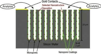
Figure 1: Schematic representation of PS sensor system. Reprinted from J. L. Gole, S. Ozdemir, Nanostructure Directed Physisorption vs. Chemisorption at Semiconductor Interfaces: The Inverse of the Hard-Soft Acid-Base (HSAB) Concept, Chem. Phys. Chem. 11, Copyright © 2010 WILEY-VCH Verlag GmbH & Co. KGaA, Weinheim [29].
We provide examples of this ready deposition in Figures 2-4. Note that the deposition does not require time consuming and costly self-assembly or the application of costly and time-intensive lithographic assembly. The nanostructured island sites once deposited to the interface are sustained on that interface in the size range 10-30 nm with no evidence for sintering. We require only that the concentration of the nanostructures be maintained at a level so as to avoid cross talk between these structures which will degrade the conductometric response of the interface. In other words, there is an optimum deposition concentration for each nanostructure deposition. However, the deposition process requires no additional control and does not demand that the nanostructured islands be placed precisely at the same points in the micropores. This simplicity of design follows a process that is much more energy efficient than is thin or thick film design. With this form of interface preparation, we provide ready reproducibility, a factor that is not easily obtained in film preparation.
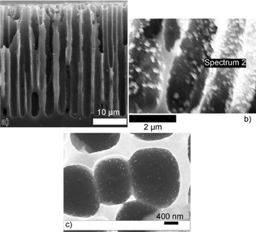
Figure 2: a) Close-up side view of p-type porous hybrid porous silicon (PS) film. [Scale bar corresponds to 10 mm.] b) Nanoparticle tin-oxide coating on PS micropores. c) 10–30 nm AuxO nanostructure deposits. Reprinted from J. L. Gole, S. Ozdemir, Nanostructure Directed Physisorption vs. Chemisorption at Semiconductor Interfaces: The Inverse of the Hard-Soft Acid-Base (HSAB) Concept, ChemPhysChem, 11, Copyright © 2010 WILEY-VCH Verlag GmbH & Co. KGaA, Weinheim [35].
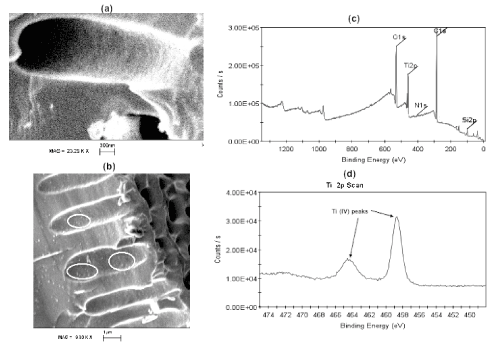
Figure 3: (a) SEM image of undecorated n-type PS pore structure. The pore is approximately one micron in diameter and 4 microns in length. (b) SEM image of porous silicon structure deposited with TiO2. Some of the TiO2 nanostructures (10-20 nm) are encircled in white. (c) XPS spectrum for the decorated porous structure showing the overall XPS spectrum including background peaks and (d) close-up of Ti 2p XPS region. Those nanostructures can be subsequently nitridated to form TiO2-xNx. Reprinted from W. Laminack, J. L. Gole, Light Enhanced Electron Transduction and Amplified Sensing at a Nanostructure Modified Semiconductor Interface, Advanced Functional Materials, 23 Copyright © 2013 WILEY-VCH Verlag GmbH & Co. KGaA, Weinheim [13].
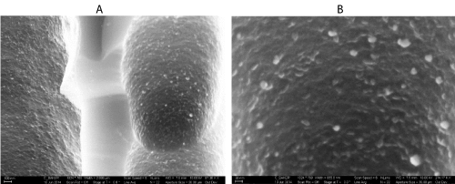
Figure 4: (a) SEM image of thiol treated TiO2 decorated porous silicon at 87.36 KX magnification (b) SEM image of thiol treated TiO2 decorated porous silicon at 274.17 KX magnification. The lighter images in the micrographs correspond to sulphur-based moiety functionalized titanium oxide. Reprinted from W. Laminack, C. Baker, J. L. Gole, Sulphur-Hz(CHx)y(z˭0,1) Functionalized Metal Oxide Nanostructure Decorated Interfaces: Evidence of Lewis Base and Brönsted Acid Sites - Influence on Chemical Sensing, JMC A. Submitted [9].
Counter to traditional metal oxide systems, the dispersed nanostructured metal oxides on PS do not operate at high temperature. Therefore, they are more energy efficient and respond more rapidly due to their dispersed nature. Our room temperature operative design, adds considerable flexibility not possible in a singly or multiply “coated” metal oxide interface. As metal oxide sensors need to operate at elevated temperatures, a power consuming heating element must be provided with the sensor housing. In several applications it is necessary to tightly control the temperature of the sensor element. This is intimately tied to the correct identification of the gas of interest. Distinguishing one gas from another requires that the heating element and sensor be well separated (channel) from the remaining electronics. This means that this configuration can be greatly affected by an impinging combustion or flue gas, rendering difficult the correct identification of gaseous species in the flow. In contrast, the PS sensor configuration depicted in Figures 1 consumes less power as it does not require the complexity of a system separated sensor/heater configuration. However, again in contrast to traditional metal oxide systems, the PS sensor depicted in Figure 1 can be extended in a heat sunk configuration to probe elevated temperature environments. This suggests that it might be used to monitor high temperature flue gas flows [5]. Figures 5, 6, 7, and 8 provide an indication of the conductometric responses observed for several nanostructure directed systems.
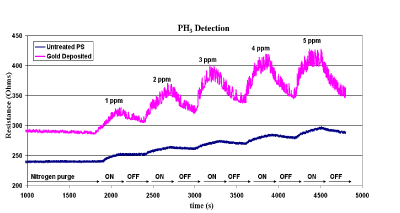
Figure 5(a): Improved response of a basic analyte, PH3, to a p-type PS sensor with an electroless AuxO coating. Here, 1,2,3,4, and 5 ppm of PH3 is pulsed onto the sensor surface every 300s. A p-type sensor is used as the gold clustered oxide deposition enhances the response of the un-treated porous silicon interface by a factor of five. Reprinted from J. L. Gole, S. Ozdemir, Nanostructure Directed Physisorption vs. Chemisorption at Semiconductor Interfaces: The Inverse of the Hard-Soft Acid-Base (HSAB) Concept, Chem. Phys. Chem. 11, Copyright © 2010 WILEY-VCH Verlag GmbH & Co. KGaA, Weinheim [35].
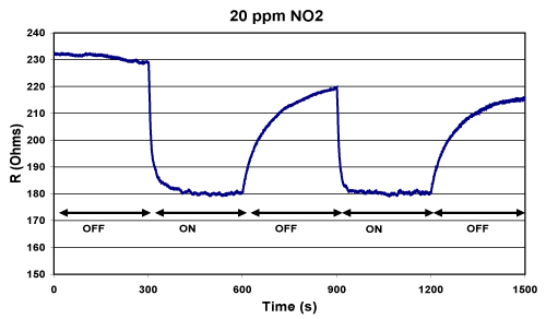
Figure 5 (b): Response of an acidic analyte, NO2, to a p-type PS sensor. Conductivity increases upon exposure to the moderate acid. The return to baseline is not complete at this concentration as NO2 sticks to the surface in this open experimental configuration. Reprinted with permission from S. Ozdemir, T. Osburn, J. L. Gole, Nanostructure Modified Gas Sensor Detection Matrix for NO Transient Conversion of NO to NO2, Journal of the Electrochemical Society. 158 (2011) J201-J207 [7].
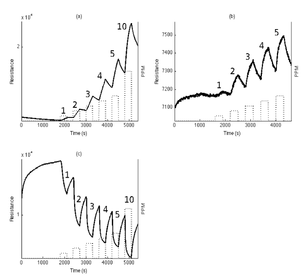
Figure 6. Resistance response of n-type porous silicon sensors to 1-5 ppm and 10 ppm of (a) NO2, (b) NO and (c) NH3. NO2 acts as a moderate acid, NO as a weak acid (resistance increase), and NH3 as a strong base (conductance increase). Compare the results for NH3 those for PH3 (Figure 5(a)). Reprinted with permission from S. Ozdemir, T. Osburn, J. Gole, Nanostructure Modified Gas Sensor Detection Matrix for NO Transient Conversion of NO to NO2, Journal of the Electrochemical Society. 158 (2011) J201-J207 [32].
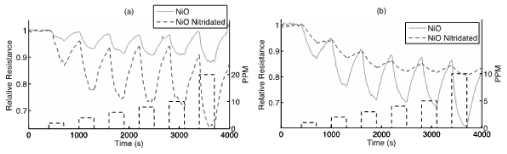
Figure 7: Response to NH3 (a) and NO (b) of a NiO treated PS interface before (solid gray) and after (dotted gray) a nitridation of the surface for 15 seconds with triethylamine. The boxes (black dashes) denote the analyte concentration from 1 to 10 ppm over the time of analyte gas exposure to the sensors. A rapid response is observed at each concentration. For NH3, nitridation produces an increase in the interface response as monitored as an increase in conductance (decrease in resistance); however, for NO the nitridation decreases the interface response. These responses are explained by the IHSAB concept. Reprinted by permission from W. Laminack, J. L. Gole, Direct In Situ Nitridation of Nanostructured Metal Oxide Deposited Semiconductor Interfaces: Tuning the Response of Reversibly Interacting Sensor Sites, ChemPhysChem, Copyright © 2014 WILEY-VCH Verlag GmbH & Co. KGaA, Weinheim [33].
The sensitivity obtained for the conductometric responses in Figures 5-8 not only is greater than that for a typical metal oxide deposition but also compares very favorably with other modes of detection. X-ray Photoelectron (XPS) spectra taken for the nitridated and sulphur functionalized PS interfaces are sensitive to 0.1%. The typical time frame for the depositions used to obtain the conductometric data in Figures 7 and 8 is 15-30 seconds. To obtain the XPS data we use deposition times which are at least 5 minutes. This corresponds approximately to an order of magnitude increase in concentration to generate signals in the 0.1% range. This indicates the significant sensitivity of the conductometric sensor responses. The magnitudes of the observed reversible interactions are described by the developing IHSAB model.
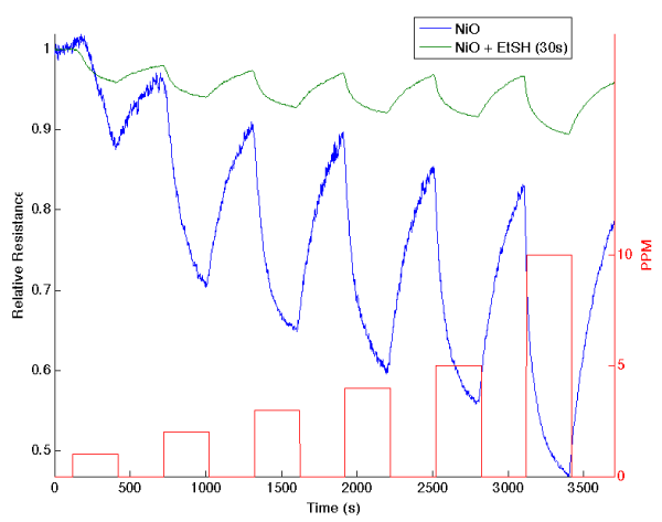
Figure 8: (a) Response of ethanethiol treated nickel oxide nanostructure deposited porous silicon (PS) interface to NH3 (a) exposure for 30 seconds and (b) exposure only to nickel oxide. The treated interface is more acidic than the NixO treated PS acidic sites after a 30 second exposure (increase in conductance). The boxes denote the analyte concentration from 1 to 10 ppm from the beginning of the gas introduction to the end. A rapid response is observed at each concentration. These responses are explained by the IHSAB concept. Reprinted with permission from W. Laminack, C. Baker, J. L. Gole, Sulphur-Hz(CHx)y(z˭0,1) Functionalized Metal Oxide Nanostructure Decorated Interfaces: Evidence of Lewis Base and Brönsted Acid Sites - Influence on Chemical Sensing, JMC A [9].
Inverse Hard/Soft Acid/Base Concept
By depositing metal oxide nanostructure islands to the PS interface, shown schematically in Figure 1, the response of the sensor can be enhanced or diminished [32]. The Inverse Hard/Soft Acid/Base (IHSAB) model, explains this phenomenon by linking chemical selectivity and the balance of electron transduction and chemisorption [5,31-33] with the sensor response mechanisms. The IHSAB model predicts the interaction of acidic, basic, and amphoteric gas analytes with the nanostructure treated PS sensor interfaces. Table 1 provides an outline of the Hard/Soft identification of acids and bases. A hard acid will form a strong ionic bond with a hard base and a soft acid will form a strong covalent bond with a soft base. For the purposes of chemical sensing, we wish to minimize this bond formation [36-38]. The IHSAB model directs the fabrication of a nanostructure-treated PS gas sensor that behaves to stimulate an electron transduction physisorption-dominated mode as an inorganic gas analyte interacts with a decorated interface. Electron transduction dominates chemisorption, through the interaction of a hard acid and soft base or soft acid and hard base. There are different ways to control the size of the interaction of those molecules that are to be sensed with variably doped metal oxide nanostructure deposited sensing interfaces. However, the dominant factor is the HOMO-LUMO energy increment. If the donor orbital energy (highest occupied molecular orbital, HOMO) is not well matched with the acceptor (lowest unoccupied molecular orbital, LUMO), then the interaction will be weak. As the HOMO (donor)-LUMO (acceptor) energy gap decreases, there can be more charge transfer between the molecule (analyte) and the created interface, leading to a stronger Lewis acid-base interaction. Conversely, the greater the HOMO-LUMO energy gap, the greater the orbital mismatch, enhancing the electron transduction mode. The IHSAB principle is in large part based on controlling the size of the Lewis acid-base bond dissociation energy.
Table 1. Sampling of Hard/Soft Acid/Base designation of various materials[22,29].
|
Hard |
Borderline |
Soft |
Acids |
H+, Li+, Na+, K+
Be2+, Mg2+, Ca2+
Cr2+, Cr3+, Al3+
SO3, BF3, Sn4+, Ti4+
|
Fe2+, Co2+, Ni2+
Cu2+, Zn2+, Pb2+
SO2, BBr3, Sn2+
NO2 |
Cu+, Au+, Ag+, Tl+, Hg
Pd2+, Cd2+, Pt2+, Hg2+
BH3 |
Bases |
F-, OH-, H2O, NH3
CO32-, NO3-, O2 |
NO2-, SO32-, Br-
N3-, N2, H2S
C6H5N, SCN |
H-, R-, CN-, CO, I
SCN-, R3P, C6H5
R2S |
The estimated positions of deposited nanostructures and gas analytes on the IHSAB scale are shown in Figure 9 relative to PS. As dictated by the scale and following the IHSAB model of interactions, PS deposited with AuxO nanostructures will produce the largest response to NH3 and PS deposited with TiO2 will produce the largest response to CO. Within the IHSAB framework, metal/metal oxide nanostructure depositions can be selected for the PS sensor interface to create a predictable range of sensitivities for various gases [5,31-33]. The relative responses have observed for select n-type and p-type systems. The analyte response data forms the basis for the development of this materials positioning diagram based largely on the interaction of the acidic metal oxides ranging from TiO2 to AuxO (x>>1) and the bases NH3 to CO.
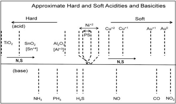
Figure 9: IHSAB scale and estimated hard and soft acidities and basicities based on resistance changes relative to a p- and n-type PS interface Reprinted by permission from W. Laminack, J. L. Gole, Nanostructure-Directed Chemical Sensing: The IHSAB Principle and the Effect of Nitrogen and Sulfur Functionalization on Metal Oxide Decorated Interface Response, Nanomaterials. 3 (2013) 469-485 [31].
It is appropriate that we compare the outlined nanostructure directed interface with other metal oxide-based systems. While it is possible to create an exhaustive list of these sensor systems, this information can be obtained from several reviews in the literature [39-43]. Because SnO2 and ZnO have been workhorses of the metal oxide sensor community we summarize a number of recent applications to the detection of several of the analytes that we have indicated in the Introduction. H2S, NH3, and CO have recently been detected using CuO thick films and nanowires. These results provide a comparative but by no means exhaustive list. For these analytes, concentrations at the sub-ppm level can be routinely measured at room temperature using the configuration of Figure 1 (LEL (Lower Exposure Limit) = 0.94ppm for H2S [44], 0.84 ppm for SO2, < 0.5 ppm for NO2, 1ppm for CO,< 0.5 ppm for NH3 with the low ppb range readily accessible, and < 0.5 ppm for PH3 ( amenable to extension to the ppb range)) [2,44-48]. The LEL’s that we quote here correspond to the lowest measured concentration directly accessible to our measurements, in the linear regime of response, with no extrapolation. Thus the quoted LEL’s are all upper bounds. Table 2 demonstrates that virtually all metal oxide systems operate at elevated temperatures. Further, processes that create thick film sensor elements, while sensitive, display significant response times, which can be on the order of minutes (vs. seconds) [30].
Table 2. Lower exposure limit of various gas sensor materials and methods.
Gas |
Gas Concentration Lower Exposure Limit (LEL) |
Response sensitivity |
Operating Temperature |
Material |
Method |
Author |
H2S |
1 ppm |
5900a |
200 C |
Ag (8 nm)-doped SnO2 |
DC magnetron sputtering (SnO2); Ag film coating |
Jin et al. [49] |
H2S |
3 ppm; 1 ppm LEL |
40%b; unreported |
74 C |
Ag-doped SnO2 |
Polymeric sol-gel |
Gong et al. [50] |
H2S |
2.5 ppm |
~85%b |
400 C |
SnO2 |
Spray pyrolysis |
Griessler et al. [51] |
H2S |
0.5 ppm |
~1.4a |
300 C |
SnO2 |
Flame spray pyrolysis (FSP) (nanopowders);
Spin coating (sensor) |
Liewhiran et al. [52] |
H2S |
10 ppm |
~1.45a |
300 C |
CuO |
Heating in open-air high purity copper foils (nanowires) |
Shao et al. [53] |
H2S |
1 ppm |
~ 5e |
25 C |
PS untreated |
Nanopore covered µ-pores |
Lewis et al. [44] |
SO2 |
50 ppm |
~40%b |
300 C |
SnO2 |
Spray pyrolysis |
Griessler et al. [51] |
SO2 |
20 ppm |
~3.8a |
300 C |
SnO2 |
FSP (nanopowders)
Spin coating (sensor) |
Liewhiran et al. [52] |
SO2 |
5 ppm |
~45%b |
350 C |
0.15 wt% V2O5/SnO2 |
Simultaneous
precipitation technique (nanopowder); painting (sensor) |
Das et al. [54] |
SO2 |
1 ppm |
~ 5e |
25 C |
PS untreated |
Nanopore covered µ- pores |
Lewis et al. [44] |
CO |
50 ppm |
8a |
350 C |
0.2 wt% Pt/SnO2 |
FSP (nanopowders);
Thermophoresis (sensor) |
Mädler et al. [55] |
CO |
500 ppm |
N/Ac |
200 – 400 C |
SnO2 |
FSP (nanopowders);
Drop coating (sensor) |
Sahm et al. [56] |
|
10 ppm |
N/A |
150 C |
CuO |
Soft chemistry (nanospheres);
Thick film screen printing (sensor) |
Hübner et al. [57] |
CO |
1 ppm |
~ 3e |
25 C |
PS, SnO2 treated |
Sn electroless solution |
DeBoer et al.
[2] |
NO2 |
5000 ppb |
20a |
220 C |
SnO2 |
FSP (nanopowders); Drop coating |
Sahm et al. [56] |
NO2 |
< 500 ppb |
~ 10e |
25 C |
PS, TiO2 treated |
TiO2 nanoparticle solution doped nanopore covered µ-pores |
Laminack et al. [45] |
NH3 |
100 ppm |
3.1a |
200 C |
CuO |
Heating in open-air high purity copper foils (nanowires) |
Shao et al. [53] |
NH3 |
<500 ppb |
~ 50e |
25C |
PS, AuxO
treated |
Au electroless solution |
Ozdemir et al. [46] |
PH3 |
<500 ppb |
~ 10e |
25 C |
PS, AuxO
treated |
Au electroless solution |
Ozdemir et al. [46,47]
Laminack et al. [48] |
H2S |
50 ppb |
N/A |
25-200C |
ZnO |
Nanorods |
Wang et al. [58] |
H2S |
1ppm |
N/A |
RTd |
In2O3 |
Nanowires
2-3 min response |
Zeng et al. [59] |
NH3 |
10 ppb |
(N/A) |
RT |
W18O49 |
Ultrathin (5nm)
Nanowire bundles |
Zhao et al. [60] |
NH3 |
100ppb
|
N/A
|
300C
|
SnO2
|
Coupling SnO2 nanowire to MEMS microhotplate
|
Meier et al. [61] |
CO |
100 ppb (Quote <5ppm) |
N/A
|
300C |
SnO2 |
Single nanowire |
Hernández-Ramírez et al.[62] |
H2S |
100 ppm |
N/A |
RT |
ZnO |
ZnO nanowire nanogenerator- possible self-powered gas sensor |
Xue et al. [63] |
aSensitivity = (Rair – Rgas)/Rair * 100%
bSensitivity = Rair/Rgas
cN/A = Not Available
dRT= room temperature
e from 
The data in Table 2 which relate primarily to film based configurations where grain boundaries can pose complications. The data in the latter part of the table correspond to single crystalline nanowires or nanobelts, whose study can reveal important information concerning the reaction between target analytes and metal oxide surfaces free of grain boundaries. Nanowire and nanobelt diameters are on the order of several nanometers, comparable to the Debye length. This provides a much larger sensitivity than the corresponding thin film or bulk counterparts and several of these studies suggest the possibility of sensitivities in the ppb range. On a somewhat larger scale, Liao et al. [64] in detecting H2S (100 ppm) found that thin nanorods have a much better sensing performance than thick nanorods. In extrapolation, researchers generally use the Langmuir absorption isotherm to fit the sensitivity-concentration curves of single nanowires whereas the power law, S = a + bcρ, is used to fit the concentration-sensitivity curves of film-based sensors [57]. It is to be noted that the sensitivities of single nanowire gas sensors are invariably less than nanowire film gas sensors. For most of the elevated temperature studies in Table 2, there are difficulties in assessing whether an optimum temperature has been explored. Further, researchers studying 1D nanostructures, in general, may not follow a unified limit of detection when claiming the detection limit of their gas sensor reaches some ppb or ppm level [65].
Four of the last six entries in Table 2 suggest the possibility of extension to the ppb level of detection using nanowire or nanorod configurations. These studies show future promise but are somewhat difficult to gauge. For example, while it has been suggested that Hernández-Ramírez et. al. [62] can monitor CO concentrations of 100 ppb, these authors indicate only that they can measure concentrations less than 5 ppm [66]. This is a very comprehensive study, which shows the promise for CO measurements both in dry air and at enhanced humidity levels. The results obtained by Zhao et al. [60] for NH3 are impressive, however, it should be apparent that 5nm nano-wire bundles are not easily prepared. The coupling of nanowires to a MEMS microhotplate again offers impressive results, but, however, this is again a difficult device to fabricate [64]. Perhaps the most impressive result in Table 2 is the nanowire- nanogenerator self-powered gas sensor of Xue et al. It is clear that nanostructure bundles and nanorods can play a role of increasing importance in sensor applications.
Magnetic Enhancement
We have also greatly enhanced the conductometric sensor response using small magnetic fields [12]. Small magnetic fields are found to greatly enhance the reversible room temperature conductometric responses of n and p - type porous silicon (PS) interfaces, treated with nanostructured island sites containing paramagnetic Co(II) and Fe(II). At concentrations sufficiently low to avoid cross talk between the nanostructured island sites, the response to NO concentrations demonstrates the significant effect which the Co(II) and Fe(II) have on the decorated extrinsic semiconductor majority charge carriers as they direct a dominant electron transduction process for reversible electron transduction and chemical sensing (IHSAB principle) in the absence of significant chemical bond formation. Co(II) and Fe(II) oxide sites enhance response and provide a means for small magnetic fields to interact with and enhance the sensor interface response. For p-type systems, the interaction is with small virtually constant thermal electron populations lying above the Fermi energy at 0° K. The electron removal rate increases with magnetic field strength. At the highest magnetic fields and NO analyte concentrations the available electron population is depleted, and the response to the analyte decreases at higher concentrations. At lower magnetic fields (<1000G) the response faithfully follows concentration. For n-type systems, the magnetic field interaction increases increases resistance. This increase in response may be attributed to the interaction with donor levels ~ 0.025 eV below the conduction band. A substantial enhancement of sensor response relative to that for the Co(II) and Fe(II) treated PS interfaces is observed, with the introduction of a small magnetic field greatly increasing an already enhanced conductometric response. [12]
Examples of Selective Monitoring
The capabilities of the porous silicon sensor are extended by providing an array of sensors with different nanoporous coatings. The selective response to each gas is based upon IHSAB theory [2,7,35,67]. A number of papers review the capabilities of porous silicon (PS) sensors [35,47,67,68]. The selection of these nanostructured metal oxide island coating provides a reversible interaction they introduce is dictated by the newly developed IHSAB model. A correctly developed porous interface sensor has several attributes. Typical sensitivity matrices for different metal oxide coatings on p-type PS sensors are shown in Table 3. These depositions create a degree of selectivity
Table 3: Increase in the signal for p-type silicon for various analyte gases relative to an undecorated PS surface after decorating with different metal oxide nanoparticles [32,35,67].
|
Tin(SnO2) |
Nickel (NiO) |
Copper (CuxO) |
Gold (AuxO) |
PH3 |
2 |
2.5 |
4 |
5 |
NO |
7-10 |
3.5 |
1 |
1.5 |
NH3 |
1.5 |
(1.5-2) |
(2-2.5) |
≈3 |
SO2 |
4 |
2 |
1+ |
2 |
Asthma Attacks
A typical example of a mixed gas configuration involves NO, NH3, and NO2. These gases (note Table 3) represent important constituents in breath, which can play an important role in asthmatic conditions. During an asthmatic attack the concentration of NO builds rapidly and can interact with O2 to produce NO2. NO contributes electrons to a p-type interface causing a significant rise in the conductometric resistance. In contrast, NO2 interacts to withdraw electrons and cause a significant increase in conductance associated with a decorated PS interface. In concert through a simple sensor array this behavior can form an early means of signalling an asthmatic attack. During these attacks, concentrations of NH3 are also signatures of a severe asthma attack. A simple device to monitor all three of these gases is therefore of importance.
Table 4. ∆R(coating)/∆R(uncoated) values are shown for H2S impedance changes on p-type extrinsic semiconductor interfaces. Comparison is to an uncoated p-type PS sensor. The nanostructured coatings deposited to the PS surface are indicated in the Table. Base resistance of the sensors used in these experiments varies from 300 to 600 Ω [69].
|
PSi substrate |
TiO2 |
SnO2 |
NiO |
AuxO |
H2S |
1 |
60 |
22 |
2 |
1200 |
PH3 is known to play an important role in the detection of METH laboratories and Figure 10 demonstrates distinct responses which can be used in an array-based format to detect this important analyte.
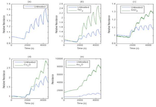
Figure 10: Comparison of responses to 2,3,4,5, and 10 ppm PH3 for (a) a PS interface consisting of an untreated p+-type surface with those treated with (b) TiO2 (c) SnOx, (d) CuxO, and (e) AuxO fractional nanostructured island depositions. PH3 was pulsed onto the interfaces (a-e) with a 300s half cycle followed by a 300s half cycle UHP nitrogen cleaning. In all cases the introduction of PH3 leads to a significant decrease in resistance which is enhanced with the introduction of nanostructure fractional depositions. The system was purged with UHP nitrogen for 1800s before operation [48].
Different responses are observed with the p-type PS sensor depending upon select metal oxide nanoparticle coating. Figure 11 demonstrate that tin oxide and gold clustered oxide nanostructured sites can be readily used to provide distinct responses to hydrogen sulfide compared to the untreated PS interface. While the data in Figures 10 and 11 demonstrate responses for p-type systems, completely distinct and complementary data has been obtained for decorated n-type semiconductors. This combination greatly enhances sensitive as selective responses can be used in a PS sensor array.
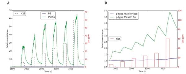
Figure 11: (A) Response of AuxO treated porous silicon (p-type) interface (green) to H2S and comparison to untreated PS interface (blue). A rapid response is observed at each concentration. The PSi interface is exposed to SnO2 for 15 seconds. The boxes (red) denote the analyte concentration over the time of analyte gas exposure to the sensors. A rapid response is observed at each concentration, but the time frame for the H2S to desorb from the sensor surface clearly exceeds the time scale for absorption (see text for discussion). (B) Response of an SnO2 treated porous silicon (p-type) interface (green) to H2S and comparison to untreated PS interface (blue). A rapid response is observed at each concentration and the response is maintained unchanged for extended periods counter to the degradation in typical H2S sensors.The PS interface is exposed to AuxO for 15 seconds. The boxes (black and red dashed) denote the analyte concentration over the time of analyte gas exposure to the sensors. A rapid response is observed at each concentration and the recovery is rapid leading to a nearly constant baseline [69].
Selective Monitoring of H2S, SO2, NH3, and NOx in presence of BTEX compounds
We have also demonstrated the highly selective detection the inorganics NO, NO2, SO2, and H2S in the presence of the BTEX contaminants toluene, benzene, and xylene using nanostructure metal oxide decorated interfaces. This selectivity can be obtained for sensors whose sensitivities are varied for a diversity of nanostructured metal oxides are applied to a porous silicon (PS) interface. Here the data focuses on NOx SO2 and H2S Figure 12. In all cases, the response to these inorganic analytes strongly dominates that for toluene, benzene, and xylene. The responses are also consistent with the recently developing Inverse Hard/Soft Acid/Base concept. The nanostructure metal oxide decorated PSi conductometric sensors are found to have selectivity ratios well in excess of 104:1 for toluene and benzene, and well in excess of 103:1 for xylene. The dominance of the response of these small inorganic sulfur and nitrogen compounds has important implications for the monitoring of significant contaminants associated with the venting and flaring of environments in the vicinity of natural gas pits as they can be present in oil and gas formations. We also know what effects of gases are on each other, (see paper on mixed gas response [15]). Counter to other sensor system the PSi sensors seem impervious to H2S gas [70].
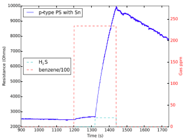
Figure 12: Comparison of response for ∼20,000 ppm benzene over the range denoted by the red box and 20.98±0.51 ppm H2S over the range denoted by the aqua box for an SnOx-decorated p-type PS sensor [70].
Sensor Rejuvenation
If a sensor is poisoned due to contamination or extensive exposure to a deleterious component of a gas mixture, which might be a strong acid, it is advantageous to have available a rejuvenation process. In most cases the rejuvenation of a sensor is difficult, at best; however, the simple open structure inherent to the porous silicon sensor facilitates this process. Figure 13 demonstrates the results of a straight-forward and repeatable rejuvenation process that can be applied to poisoned sensors [46]. This facilitates their cycling and decreases the long-term expense of a sensor device.
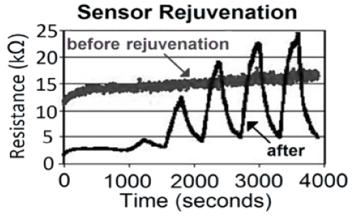
Figure 13: Response to NH3 after a sensor is subjected to a rejuvenation process. The contaminated sensor response is in grey, the rejuvenated sensor response is in black [46].
Extension to Mixed Gas Sensing
We have established models for the interaction of gases on decorated porous silicon interfaces. Mixed gas analytes interact with nanostructure decorating metal oxide island sites supported on a microporous silicon substrate. The Inverse Hard/Soft acid /base (IHSAB) concept is used to assess a diversity of conductometric responses for mixed gas interactions as a function of these nanostructured metal oxides. The IHSAB framework allows us to understand the nonlinear interactions of the analyte gases as shown in Figure 14.
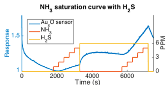
Figure 14: AuxO deposited p-type interface response to an NH3 / H2S mixture. The interface is allowed to come to a base line after treatment for 1800 s of UHP N2. NH3 is slowly added to the decorated interface. Once the initial NH3 exposure ceases, H2S is exposed to the surface and is allowed to equilibrate. The NH3 is slowly added again to the interface. The response of the to NH3 is greater with the H2S background [15a].
We have developed the first phase of a means of characterizing mixed gas interactions. The sensor response to the various analytes depends on other analytes present. This process is dictated by the IHSAB model which can be use to evaluate compound interactions. An example of this process is provided in Figure 14 where the interactions of NH3 and H2S influence each other in a manner that can be evaluated in the IHSAB framework. One analyte response on the sensor must be taken into account to describe a second analyte response. This change in response for a sensor depends on whether the sensor is an n or p type semiconductor and the Lewis acidic (or basic) nature of initial analyte gas. However, these modifications are well represented using a combination diffusion/absorption–based model for multi-gas interactions where a newly developed response absorption isotherm, based on the Fermi distribution function is applied. A further coupling of this model with the IHSAB concept describes the considerations in the modelling of multi-gas mixed analyte-interface, and analyte-analyte interactions.
Taking into account the molecular electronic interaction of both the analytes with each other and an extrinsic semiconductor interface we demonstrate how the presence of one gas can enhance or diminish the reversible interaction of a second gas with the extrinsic semiconductor interface. We can easily model multigas interaction for an array of metal oxides as shown in Figure 14. These concepts demonstrate important considerations in the array-based formats for multi-gas sensing and its applications [15].
Initial detailed modelling suggests that we can easily extract analyte concentrations from a mixed gas. Results from a simple simulation are shown in Figure 15. Here a linear interaction of a variety of mixed analyte gases is simulated [15 a,b]. We simulate the response of two sensors which are deposited with different metal oxide nanoparticles. These nanoparticles cause the two sensors to have differing responses for the two analyte gases. The resulting simulated responses Figure 16 are then processed through an algorithm to extract the concentrations of the mixed gases. This computed concentrations are then compared to the input concentrations of the simulation Figure 16. A simple algorithm allows for extremely accurate prediction of concentrations.
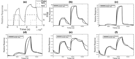
Figure 15. Response of p-type (a)uncoated (b) PS/TiO2 (c) PS/AuxO (d) PS/MgO (e) PS/Ca and (f) PS/Ba interfaces to 5 ppm of NO (0-300 sec), NH3 (900-1200 sec) and NO and NH3 simultaneously (300 – 600 sec and 1200-1500 sec) compared to the simulated response. Note that the response of the mixed gas levels off to a specific value independent of which gas was exposed to the sensor first [15].
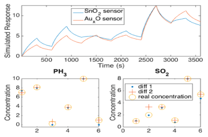
Figure 16: Extracted gas concentrations from the simulated response. Gas simulations of two sensors without any noise are presented at the top. The extracted concentration vs the actual concentration is seen at the bottom of the two simulated gases. Diff 1 represents the extracted concentration using only the first derivative of the response while Diff 2 represents the extracted concentration using the second derivative [15a].
Power Consumption
We have examined the IV response associated with the Porous Silicon sensor substrates, testing for linearity and bias. Figure 17 below shows the IV curves obtained for the operating sensor of Figure 1. We demonstrate forward and reverse scans for recently produced sensors which feature linearity over the entire testing range as well as no bias. Based on the linear IV curve, the continuous power consumption is between 25 and 60 microwatts/second over the range 1 to 1.5 volts. We compare this result to the results of Ahlers et al. [71] Figure 18. The IV curves in Figure 17 in concert with the analysis of Ahlers et al. [71] Figure 18 demonstrate that the nanostructure directed sensor systems require considerably less power for operation than do thick or thin film sensors. Mueller et al. [72] following Ahlers et al. [71] have recently discussed a MEMS toolkit for metal oxide based sensing systems. Using silicon micromachining technologies they have developed metal oxide gas sensor elements with very small heat consumption. The power of a single micromachined sensor element is found to be an order of magnitude less Figure 18 than that of thick film devices. In their Table 1, these authors quote heating powers, and necessary overhead heating requirements which sum to 1 to 1.5 Watts for a Thick-film sensor (column 1-Figure 18) and 0.4 to 0.6 Watts (0.8 Watts including sensor) for a micromachined sensor array. The required power for the nanostructure directed PS systems we have considered is virtually in the noise level of Figure 10. For this reason they are not shown in Figure 18. We emphasize that the described system competes quite favorably with those micro-machined sensor systems whose construction may be more costly and time consuming.

Figure 17: IV curves for continuous sensor response.
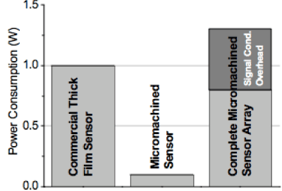
Figure 18: A comparison of power consumptions. A full-fledged micro- machined sensor array with heater driver requires as much power as a single commercial thick film device. Additional power for signal conditioning electronics for a micro-machined sensor array is also indicated. Reprinted by permission from S. Ahlers, P. Kreisl, G. Müller, A Low-Power Metal-Oxide Based Gas Sensing System, 203rd ECS meeting, paper 2873, April 28, 2003, The Electrochemical Society [71].
The data that we have summarized indicate a novel mode to create metal oxide sensors with significant ease that facilitates the development of reversible conductometric sensor systems. These are energy efficient, forgiving systems. Our controlled deposit of metal oxide sites eliminates the need for thin (or thick) films. The process enhances diffusion time and facilitates ease and repeatability of construction. Rapidly responding, reversible, room temperature sensors have been created and evaluated for the detection of various inorganic gas analytes at low ppm to ppb concentrations. These sensors are more energy efficient, since they do not require elevated temperatures to operate and can be heat sunk to operate at elevated temperatures. In addition, they respond more rapidly due to their dispersed nature. The sensors can be constructed using easily accessible solution based sources. This suggests that their scalability is eminently possible and multiple sensor configurations have already been constructed. Within the framework dictated by the IHSAB model, select metal oxide nanostructures have been deposited to the PS interface, to create an array of sensitivities to a variety of gas analytes. The in-situ nitridation of metal oxide islands deposited to the PS interface extends the array, allowing greater flexibility for tuning the sensor response. The changes in response behavior are explained largely by the developing IHSAB concept.
Future Considerations
Future work required for the development of these sensors should focus on the goal of extracting sensor data from arrays of differently coated sensors. Since the sensors are easy to create and the nanoparticle depositions are not labor intensive, it’s relatively simple to produce a sensor array. These sensors have correlated responses to the analyte gases allowing us to quickly extract relevant information. The arrays should be made up of the widest variance of the nanoparticles. We have demonstrated success in separating the various gas signals using a two-sensor array of Sn and Ag treated sensors. These two metals were chosen since they differ widely in their Lewis acidity allowing a test to be run on two different gases [15a]. Other more complicated arrays could be created to both minimize the noise and simplify the ease of signal extraction.
While the sensors we created easily detect the analytes at lower ppm, the research has focused on creating a variety and range of sensor sensitivity. Future research should use more tightly defined doping levels for the silicon wafers used in the etch process. The increase in uniformity will enhance the extraction of data from array outputs, by eliminating any random bias in the array. We have also considered information retrieval. Primarily we have extracted information from the sensor data by simple model fitting. The basic physics of diffusion and absorption dominate the measured response and are easily modelled. We have generated simulations of the analyte of interest interacting with the sensors and fit the actual sensor data to extract the value of the response. However, the sensor fitting is not linear and small amounts of noise could drastically affect the sensor response. Future work could be used to build upon the initial fitting of the sensor data, generating a large amount of quick inexpensive focusing data to feed into a recurrent neural net and quickly extract the required data, followed with a reasonable nonlinear model.
- Al Rifai, Hejjo M, Christophersen M, Ottow S, Carstensen J, et al. (2000) Journal of The Electrochemical Society 147: 627-635.
- Lewis SE, DeBoer JR, Gole JL, Hesketh PJ (2005) Sensors and Actuators B: Chem 110: 54-65.
- Gole JL, Lewis S, Lee S (2007) Physica status solidi 204: 1417-1422.
- Kang DK, Corno JA, Gole JL, Shin HC (2008) Journal of The Electrochemical Society, 155: A276-A281.
- Gole JL, Laminack W (2012) Chemical sensors: simulation and modelling, 3: 85-136.
- Laminack W, Gole J (2015) Multi-gas interaction modelling on decorated semiconductor interfaces: A novel Fermi distribution-based response isotherm and the inverse hard/soft acid/base concept. Applied Surface Science 359: 774-81.
- Gole JL, Osburn TS (2010) Novel concept for the formation of sensitive, selective, rapidly responding conductometric sensors. ECS Trans 33: 239-244.
- Baker C, Gole JL (2014) Interface modifications of porous silicon for chemical sensor applications. JSM Nanotechnol Nanomed 2: 1021.
- Laminack W, Gole JL (2015) Sulphur-Hz(CHx)y(z?0,1) Functionalized Metal Oxide Nanostructure Decorated Interfaces: Evidence of Lewis Base and Brönsted Acid Sites - Influence on Chemical Sensing. Journal of Materials Chemistry and Physics 160: 20-31.
- Star AVJ, Skarupo S, Thomas D, Gabriel JP (2006) Gas Sensor Array Based on Metal-Decorated Carbon Nanotubes. The Journal of Physical Chemistry B 110: 21014-21020.
2021 Copyright OAT. All rights reserv
- Lang HP (1998) A chemical sensor based on a micromechanical cantilever array for the identification of gases and vapors. Applied Physics A: Materials Science & Processing 66: S61-S64.
- Baker C, Laminack W, Tune T, Gole JL (2014) Magnetically induced enhancement of reversibly responding conductometric sensors. Journal of Applied Physics 115:164312.
- Laminack W, Gole JL (2013) Light Enhanced Electron Transduction and Amplified Sensing at a Nanostructure Modified Semiconductor Interface. Advanced Functional Materials 23: 5916-5924.
- Gole JL, Baker C (2016) Optimization of PSi-based Sensors Using IHSAB Principles, in Porous Silicon: From Formation to Application, ed. Ghenadii Korotchenkov. CRC Press 45-68.
- Laminack W, Baker C, Gole JL (2015) Response Simulation and Extraction of Gas Concentrations for Nanostructure Directed Nano- /Microporous Silicon Interfaces. ECS Transactions 69: 141-152.
- Baker C, Gole JL (2016) Detection of Liquid Organic Solvents on Metal Oxide Nanostructure Decorated Porous Silicon Interfaces. ACS Sensors 1: 235-42.
- Barsan N, Schweizer-Berberich M, Göpel W (1999) Fundamental and practical aspects in the design of nanoscaled SnO2 gas sensors: a status report, Fresenius' journal of analytical chemistry 365: 287-304.
- Comini E (2006) Metal oxide nano-crystals for gas sensing. Anal Chim Acta 568: 28-40. [Crossref]
- LeGorea LJ, Lada RJ, Moulzolfa SC, Vetelinoa JF, Fredericka FJ, et al. (2002) Defects and morphology of tungsten trioxide thin films. Thin Solid Films 406: 79-86.
- Rani S, Roy SC, Bhatnagar M (2007) Effect of Fe doping on the gas sensing properties of nano-crystalline SnO2 thin films. Sensors and Actuators B: Chemical 122: 204-210.
- Jiménez I, Arbiol J, Dezanneau G, Cornet A, Morante JR (2003) Crystalline structure, defects and gas sensor response to NO2 and H2S of tungsten trioxide nanopowders. Sensors and Actuators B: Chemical 93: 475-485.
- Moulzolf SC, Ding S, Lad RJ (2001) Stoichiometry and microstructure effects on tungsten oxide chemiresistive films. Sensors and Actuators B: Chemical 77: 375-382.
- Ponce M, Aldao C, Castro M (2003) Influence of particle size on the conductance of SnO2 thick films, Journal of the European Ceramic Society 2105-2111.
- Rothschild A, Komem Y (2004) The effect of grain size on the sensitivity of nanocrystalline metal-oxide gas sensors. Journal of Applied Physics 95: 6374-6380.
- Yoon DH, Choi GM (1997) Microstructure and CO gas sensing properties of porous ZnO produced by starch addition, Sensors and Actuators B: Chemical 45: 251-257.
- Morrison SR (1987) Selectivity in semiconductor gas sensors, Sensors and Actuators. 12: 425-440.
- Watson J (1994) The stannic oxide gas sensor, Sensor Review, 14: 20-23.
- Yamazoe N, Shimanoe K, Aswal DK, Gupta SK (2007) Overview of gas sensor technology. Nova Science Publishers Inc., New York.
- Kottke PA, Federov AG, Gole JL (2009) Multiscale Mass Transport in Porous Silicon Gas Sensors, in: M. Schlesinger (Ed.). Modern Aspects of Electrochemistry 43: 139-168.
- Schechter I, Ben-Chorin M, Kux MA (1995) Gas Sensing Properties of Porous Silicon. Analytical Chemistry 67: 3727.
- Laminack W, Gole JL (2013) Nanostructure-Directed Chemical Sensing: The IHSAB Principle and the Effect of Nitrogen and Sulfur Functionalization on Metal Oxide Decorated Interface Response. Nanomaterials 3: 469-485.
- Gole JL, Goude EC, Laminack W (2012) Nanostructure-Driven Analyte–Interface Electron Transduction: A General Approach to Sensor and Microreactor Design. Chem. Phys. Chem 13: 549-561.
- Laminack W, Gole JL (2014) Direct In Situ Nitridation of Nanostructured Metal Oxide Deposited Semiconductor Interfaces: Tuning the Response of Reversibly Interacting Sensor Sites. Chem. Phys. Chem 15: 2473-2484.
- Gole JL, Laminack W (2013) Nanostructure-directed chemical sensing: The IHSAB principle and the dynamics of acid/base-interface interaction. Beilstein J. Nanotechnol 4: 20-31.
- Gole JL, Ozdemir S (2010) Nanostructure-directed physisorption vs chemisorption at semiconductor interfaces: the inverse of the HSAB concept. Chemphyschem 11: 2573-2581. [Crossref]
- Pearson RG (1990) Hard and soft acids and bases-the evolution of a chemical concept, Coord. Chem Rev 100: 403-425.
- Parr RG, Pearson RG (1983) Absolute hardness: companion parameter to absolute electronegativity. J. Am. Chem. Soc 105: 7512-7516.
- Parr RG, Yang W (1989) Density Functional Theory of Atoms and Molecules, Oxford University Press, New York.
- Wang C, Yin L, Zhang L, Xiang D, Gao R (2010) Metal oxide gas sensors: sensitivity and influencing factors. Sensors (Basel) 10: 2088-2106. [Crossref]
- Bârsan N, Weimar U (2003) Understanding the Fundamental Principles of Metal Oxide Based Gas Sensors; the example of CO Sensing with SnO2 Sensors in the Presence of Humidity, J Phys Condens. Matter 15 R813.
- Huang J, Wan Q (2009) Gas Sensors Based on Semiconducting Metal Oxide One-Dimensional Nanostructures. Sensors 9: 9903-9924.
- Korotcenkov G (2007) Metal Oxides for Solid-state Gas Sensors: What determines our choice? Materials Science and Engineering B 139: 1-23.
- Ho GW (2011) Gas Sensor with Nanostructured Semiconductor Oxide Materials. Science of Advanced Materials 3: 150-168.
- Lewis S, Gole JL unpublished results.
- Laminack W, Pouse WN, Gole JL (2012) Dynamic Interaction of NO2 with a Nanostructure Modified Porous Silicon Matrix: Acidity, Sensor Response, and the Competition for Donor Level Electrons. ECS J. Solid State Sci. Tech. 1: Q25–Q34.
- Ozdemir S, Gole JL (2008) Porous Silicon Gas Sensors for Room Temperature Detection of Ammonia and Phosphine. ECS Transactions 16: 379-387.
- Ozdemir S, Gole JL (2010) A phosphine detection matrix using nanostructure modified porous silicon gas sensors. Sensors and Actuators B 151: 274-280.
- Laminack W, Gole JL (2014) A Variable Response Phosphine Sensing Matrix Based on Nanostructure Treated p, and n-type Porous Silicon Interfaces. IEEE Sensors 14: 2731-2738.
- Jin C, Yamazaki T, Ito K, Kikuta T, Nakatani TN (2006) H2S sensing property of porous SnO2 sputtered films coated with various doping films, Vacuum 80: 723-725.
- Gong J, Chen Q, Lian M, Liu N, Stevenson R, Adami RF (2006) Micromachined nanocrystalline silver doped SnO2 H2S sensor, Sensor and Actuators. B: Chemical 114: 32-39.
- Griessler C, Brunet E, Maier T, Steinhauer S, Köck SA, et al. (2011) Tin oxide nanosensors for highly sensitive toxic gas detection and their 3D system integration. Microelectronic Engineering 88: 1779-
- Liewhiran C, Tamaekong N, Wisitsora A, Phanichphant AS (2012) The Monitoring of H2S and SO2 Noxious Gases from Industrial Environment with Sensors Based on Flame-Spray-Made SNO2 Nanoparticles. Engineering Journal 16 123-134.
- Shao F, Hernándes-Ramírez F, Prades JD, Fábrega C, Andreu T, Morante JR (2014) Copper (II) oxide nanowires for p-type conductometric NH3 sensing, Applied Surface Science. 311: 177-181.
- Das S, Chakraborty S, Parkash O, Kumar D, Bandyopadhyay S, et al. (2008) Vanadium doped tin dioxide as a novel sulfur dioxide sensor. Talanta 75: 385-389. [Crossref]
- Mädler L, Roessler A, Pratsinis SE, Sahm T, Gurlo A, et al. (2006) Direct formation of highly porous gas-sensing films by in situ thermophoretic deposition of flame-made Pt/SnO2 nanoparticles, Sensors and Actuators. B: Chemical 114: 283-295.
- Sahm T, Mädler L, Gurlo Barsan AN, Pratsinis SE, Weimar U (2004) Flame spray synthesis of tin dioxide nanoparticles for gas sensing, Sensors and Actuators. B: Chemical 98: 148-153.
- Hübner M, Simion CE, Tomescu-Stanoiu A, Pokhrel S, Bârsan N, et al. (2011) Influence of humidity on CO sensing with p-type CuO thick film gas sensors, Sensors and Actuators. B: Chemical 153: 347-353.
- Wang C, Chu X, Wu M (2006) Detection of H2S down to ppb levels at room temperature using sensors based on ZnO nanorods, Sensors and Actuators. B: Chemical 113: 320-323.
- Zeng Z, Wang K, Zhang Z, Chen J, Zhou W (2009) The detection of H2S at room temperature by using individual indium oxide nanowire transistors. Nanotechnology 20: 045503.
- Zhao YM, Zhu YQ (2009) Room temperature ammonia sensing properties of W18O49 nanowires, Sensors and Actuators. B: Chemical 137: 27-31.
- Meier DC, Semancik S, Button B, Strelcov E, Kolmakov A (2007) Coupling nanowire chemiresistors with MEMS microhotplate gas sensing platforms. Applied Physics Letters 91: 063118.
- Hernández-Ramírez F, Tarancón A, Casals O, Arbiol J, Romano-Rodríguez A, et al. (2007) High response and stability in CO and humidity measures using a single SnO2 nanowire, Sensors and Actuators. B: Chemical 121: 3-17.
- Xue X, Nie Y, He B, Xing L, Zhang Y, et al. (2013) Surface free-carrier screening effect on the output of a ZnO nanowire nanogenerator and its potential as a self-powered active gas sensor. Nanotechnology 24: 225501.
- Liao L, Lu HB, Li JC, He H, Wang DF, et al. (2007) Size Dependence of Gas Sensitivity of ZnO Nanorods. Phys. Chem. C 111: 1900-1903.
- Zhang D, Liu Z, Li C, Tang T, Liu X, et al. (2004) Detection of NO2 down to ppb Levels Using Individual and Multiple In2O3 Nanowire Devices, Nano Lett 4: 1919-1924.
- Huang J, Wan Q (2009) Gas Sensors Based on Semiconducting Metal Oxide One-Dimensional Nanostructures. Sensors 9: 9903-9924
- Ozdemir SA, Gole JL (2007) The Potential of Porous Silicon Gas Sensors. Current Opinions in Solid State and Materials Science 11: 92-100.
- Ozdemir SA, Gole JL (2010) Sensitivity Improvement and Response Time Scale of Porous Silicon Conductometric Gas Sensors. ECS Transactions 33: 111-115.
- Baker C, Laminack W, Gole JL (2015) Sensitive and Selective Detection of H2S and Application in the presence of toluene, benzene, and xylene, Sensors and Actuators, B Chemical 212: 28-34.
- Baker C, Laminack W, Gole JL (2016) Selective Detection of Inorganics NOx, SO2, and H2S in the presence of volatile BTEX contaminants, toluene, benzene, and xylene, Air Quality Atmosphere and Health 9: 411-419.
- Ahlers S, Kreisl P, Müller G (2003) A Low-Power Metal-Oxide Based Gas Sensing System, 203rd ECS meeting, paper 2873, April 28.
- Mueller G, Friedberger A, Kreisl P, Ahlers S, Schulz A, et al. (2003) A MEMS toolkit for metal-oxide-based gas sensing systems. Thin Solid Films 436: 34-45.