Recently, tremendous fundamental and technological interest has been created by the possible use of the spin degree of freedom of electrons for information processing. This field, often referred to as spintronics, is rapidly developing: new ideas and promising materials emerge, which - taking advantage of the broadening facilities of nanotechnology - offer novel sensor, memory and even logics applications. In this article we review some intriguing aspects of spin related transport at nanoscale. First the basic concept of spin polarized transport and the calculation of the current spin polarization is demonstrated in a tutorial way using the framework of the Landauer formalism. Next the experimental method of superconducting Andreev spectroscopy is reviewed, which is capable of resolving both the current spin polarization and the spin diffusion length.
spin polarization, Landauer formalism, spin valve, Andreev reflection, spin diffusion length
The spin dependence of electronic transport is hidden in most metals. However, spin polarized current injected to a nonmagnetic conductor keeps the spin memory within a certain distance, typically in the submicron range [1,2]. Building on this principle, nanoscale devices have been prepared where the size of the components is well below this distance, the spin diffusion length, and both the control of the spin states and the utilization of the spin information have been demonstrated [1-6]. In most of these electronic applications ferromagnetic components act as spin filters and detectors [7,8], while a nonmagnetic conductor mediates the spin information. For the design of such nanodevices a proper understanding of spin dependent transport is necessary, including the knowledge of the carriers' spin polarization, and the determination of the spin diffusion length.
In the first part of this review we give a tutorial introduction to spin polarized transport based on the Landauer formalism [9], widely applied in the field of nanophysics. In the second part a special measurement technique is reviewed, which allows the direct determination of the current spin polarization, and with which even the decay of the spin polarization i.e. the spin diffusion length can be determined in a nonmagnetic layer.
Spin dependent transport in nanostructures
In a macroscopic conductor, the electrons suffer numerous scattering processes as they move from one electrode towards the other. Due to the scattering on impurities and lattice defects the drift momentum of the electrons gained from the electric field is lost. This process is described by the characteristic length scale of the momentum relaxation mean free path, . Inelastic scattering processes like the scattering on lattice vibrations lead to a change of energy, which results in the loss of phase coherence for electron waves. The corresponding characteristic length scale is called phase diffusion length,
  [10,11]. Within a large enough distance the electrons also loose their spin information, as characterized by the spin diffusion length,
  [7]. In a nanostructure, however, all these length scales may become comparable to, or even larger than the characteristic size of the structure,
  For instance, in small enough structures
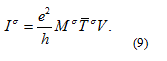
  the spin information is preserved, which is a key ingredient for spintronic applications [12]. For structures, smaller than coherent quantum mechanical features appear, whereas for
  a ballistic transport is observed, i.e. the electrons scatter only on the edges of the structure, but not inside.
Here we give a simple model to demonstrate how spin polarized current may arise in ferromagnetic nanostructures, which are smaller than the spin diffusion length. In order to provide a microscopic insight to the relevant processes we use the well-established approach of the Landauer formalism [9,11] which has been successfully applied to describe several nanoscale systems, like atomic-sized conductors [13] or semiconductor nanostructures [14,15].
As a simplified model, first we consider an ideal two-dimensional wire with parallel walls (Figure 1a). In the ballistic limit, no scattering occurs in the wire, and an electron entering the wire from one side will propagate to the other side without changing its energy and spin state. Along the wire (x-direction) the electrons exhibit a free, reflectionless propagation, whereas perpendicular to the wire (y-direction) quantized transverse modes are formed. In this simple geometry, the wave function factorizes to the product of a longitudinal and a transverse wave function, and the energies corresponding to the transverse standing waves and the longitudinal propagation are simply added. After including magnetism in a Stoner type picture the energy dispersion for this system can be written as:
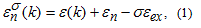
where is the energy corresponding to the quantized transverse modes,  is the dispersion of the extended Bloch states in the x direction
 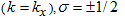 is the spin index, and
  is the exchange energy. The resulting dispersion is a set of one dimensional dispersion curves, which are vertically shifted by the transverse energies and the exchange energy (Figure 1b). The discrete one dimensional dispersions are called conductance channels [11,16].
In such an ideal wire the states with positive and negative Κ are well separated, the former are all coming from the left electrode, while the latter are all coming from the right electrode. In a symmetric situation, no net current flows. Application of a bias voltage between the two sides of the wire, however, shifts the chemical potentials of the right and left moving electron states by  with respect to each other, and this imbalance results in a finite current. For a selected conductance channel the velocity of the electrons and the density of states is respectively given as
where is the length of the nanowire. The spatial density for the electron states in the  energy window is obtained as
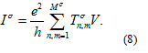
The current is then calculated as a product of charge, velocity and electron density, summing over the spins and all the conductance channels:
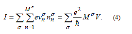
Here  is the number of open conductance channels, i.e. the number of 1D dispersion curves crossing the Fermi energy for a given spin orientation. Note that
  cancels in the product of V and n , thus the above result is valid for any shape of the dispersion curve. Furthermore, the two dimensional model only simplifies the visualization, but the above arguments also hold for any perfect three dimensional nanowire with uniform cross section along the x axis.
Here we have taken advantage of the assumption that the spin state is conserved, i.e. the structure is smaller than the spin diffusion length. This has allowed the separation of the current to a purely spin up and a purely spin down component being two independent routes of the transport: 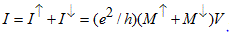 . The total current is determined by the number of open conductance channels, and the conductance
  is an integer multiple of
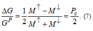
Due to the shifted spin subbands, M ↑ not necessarily equals M ↓ . This is indicated by Figure 2, where only the linearized part of the 1D dispersions around the Fermi energy is shown demonstrating that the free electron dispersions in Figure 1b are only illustrations and are generally not considered in this model. The degree of the resulting spin polarization can be characterized by the ratio of the spin polarized current and the total current:
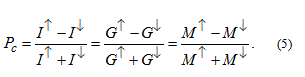
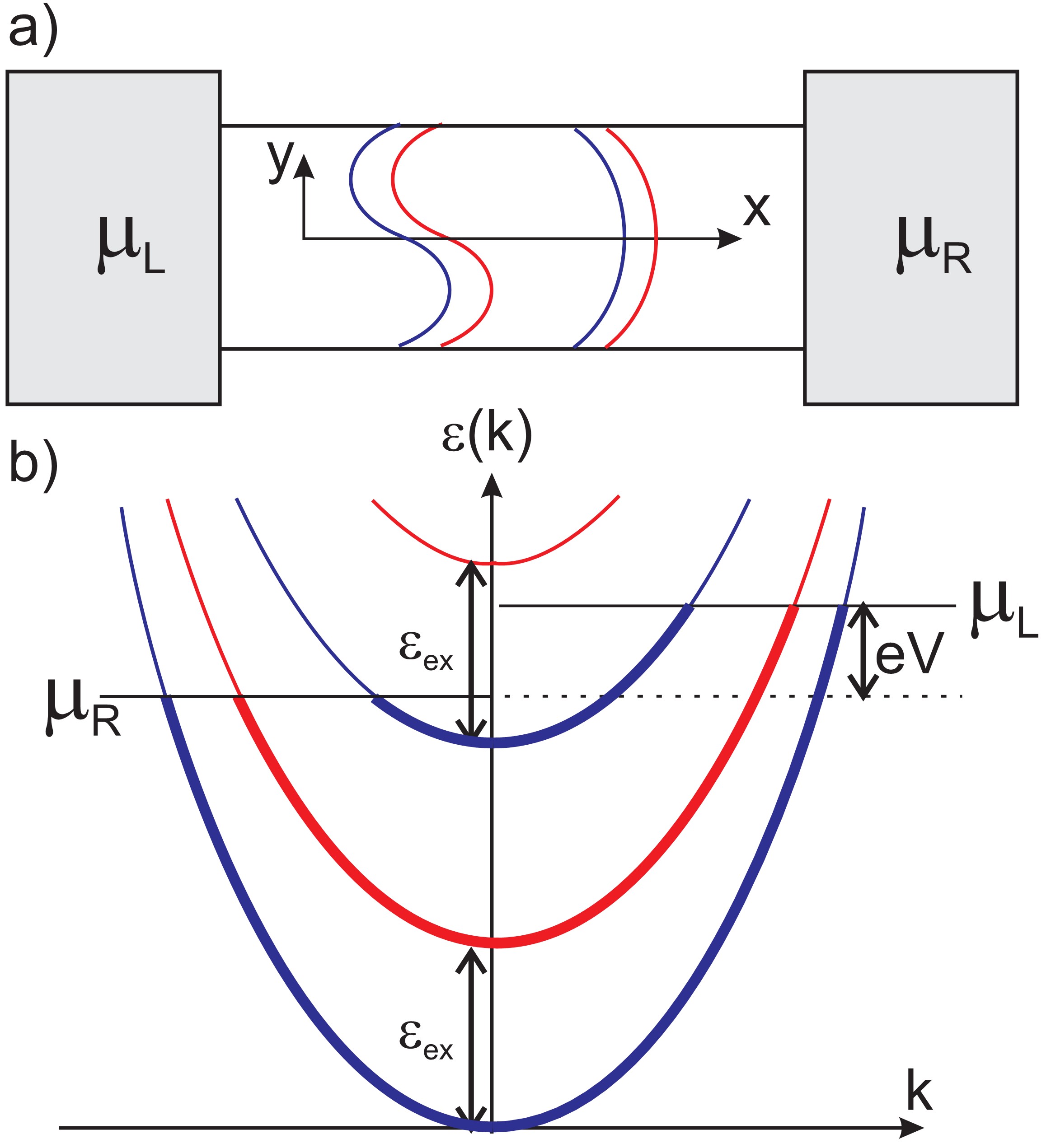
Figure 1. Panel (a) demonstrates an ideal 2D quantum wire with parallel walls and the absence of scattering inside the wire. The standing waves demonstrate the quantized transverse modes in the wire. Panel (b) demonstrates the dispersion of the conductance channels inside the wire in a free electron picture, using 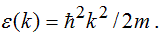 . The blue parabolas correspond to spin up electrons, whereas the red parabolas stand for the spin down electrons. The two spin subbands are shifted by an energy
  . The thick/thin lines denote the occupied/unoccupied states. Note, that right going states (k > 0) are occupied up to an energy higher by eV than the left moving states (k < 0).
This normalized current spin polarization can reach even 100% (Pc = 1) in case of a half-metal, where only one type of carrier is present at the Fermi level.
In a ballistic quantum wire with slowly changing channel width the conductance is solely determined by the number of open conductance channels in the narrowest cross section, yielding a quantized conductance increase as the quantum point contact is tuned wider [14]. It is worth noting that in the simplified context of ballistic quantum wires the introduction of an exchange coupling is similar to an effective spatial narrowing or widening of the channel, which would increase/decrease the transverse quantized energies, and finally the narrowest effective cross section determines the conductance. This is illustrated for a particular arrangement in Figure 3. The exchange coupling is switched on adiabatically in two regions resulting in either parallel (P), or antiparallel (AP) magnetization (Figure 3b and 3d). The two magnetic regions are separated by a normal part. The corresponding effective channel widths are demonstrated in panels (c) and (e) separately for spin up and spin down electrons. For electrons with majority spin direction (spin direction parallel to the magnetization direction) the number of open channels is denoted by M↑, for minority spins (antiparallel spin direction to the magnetization direction) the number of open channels is M↓ (<M↑), whereas in the normal region Mο channels are open. (Note, that here the superscript ↑denotes majority orientation instead of the real spin direction, and the number of open channels is also for down spins in down oriented magnetization of the magnetic layer.) In all cases the net conductance is determined by the number of open channels in the narrowest cross section, which is Mο for up spins in the case of parallel oriented magnetic regions (top part in panel (c)), and M↓ in all other cases. Therefore the total conductance is  i.e. the P orientation has evidently larger conductance, such that the relative conductance difference is
Figure 3. Panel (a) demonstrates the basic idea of a GMR structure: two ferromagnetic regions are separated by a narrow normal region, and this structure is connected to normal leads at both sides. Panels (b,d) demonstrate the variation of the exchange energy along the structure. Panel (b) corresponds to the parallel magnetic orientation of the layers (both layers have ↑magnetic orientation), whereas panel (d) demonstrates the antiparallel orientation (↑in the first layer and ↓in the second one). Panels (c) and (e) respectively show the equivalent ballistic model, where the change of the exchange energy is replaced by an effective narrowing or widening of the channel. In all panels blue (red) lines correspond to up (down) spin electrons.
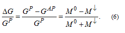
Assuming ,  a relative conductance change proportional to the spin polarization in the ferromagnetic region is obtained:
This can be considered as a ballistic toy model for the Nobel prize awarded and widely applied giant magnetoresistance (GMR) phenomenon [17,18].
A more realistic description can be given for the conductance of a piece of magnetic nanowire inserted between nonmagnetic reservoirs by taking also into account elastic scatterings (Figure 4). According to the Landauer picture the transport in this system can be be described by the transmission probabilities Tnm, i.e. the probability for the transmission of an electron from channel n on the left side to channel m on the right side. These transmission probabilities depend on the “waveguide” parameters of the wire.  While corresponds to the previous model of an ideal wire,
  represents scatterings in the wire due to defects, impurities, etc.
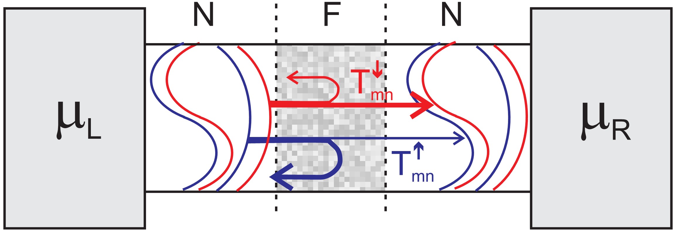
Figure 4. A diffusive ferromagnetic region is sandwiched between two normal metal ideal quantum wires. The transport is determined by spin dependent transmission probabilities between the conductance channels at the two sides.
As no spin mixing occurs between the spin up and spin down states, the current can still be calculated for each spin state independently taking into account the finite transmissions of the channels: [11,13,16]:
The values of  depend on the Fermi wave numbers of the involved channels. Due to the spin dependent shift of the dispersions the spin up and the spin down channels have different wave numbers at the Fermi energy. Thus, in general, the transmission probability may become spin dependent even without any direct spin interaction, like spin-orbit coupling.
The spin dependent current can be rewritten in the form:
where  is the average transmission probability for all the conductance channels with a given spin direction. With this notation the spin polarization of the current can be written as:
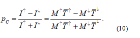
It is evident from this formula, that either the difference of the transmission probabilities for the two spin channels, or the difference in the number of open channels for spin up and spin down electrons gives contribution to the spin polarization of the current.
In case of a few conductance channels the difference in and  may introduce a spin polarized current even for the same number of open channels. Indeed, for ferromagnetic atomic point contacts, the transmission probabilities for the two spin channels are expected to differ significantly [19,20].
However, for larger structures, where many conductance channels are present (Figure 2), is an average over a broad ensemble of different wavenumbers, and for diffusive junctions random matrix theory (RMT) predicts a universal value of 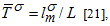 where L is the length of the diffusive region. As the momentum relaxation mean free path is expected to be similar for the two spin subbands,
  can be assumed. Accordingly, the key contribution to the spin polarization is still given by the difference of
  and . In this limit, Eq. 5 gives a reasonable approximation for the spin polarization, even for non-ideal transmission probabilities
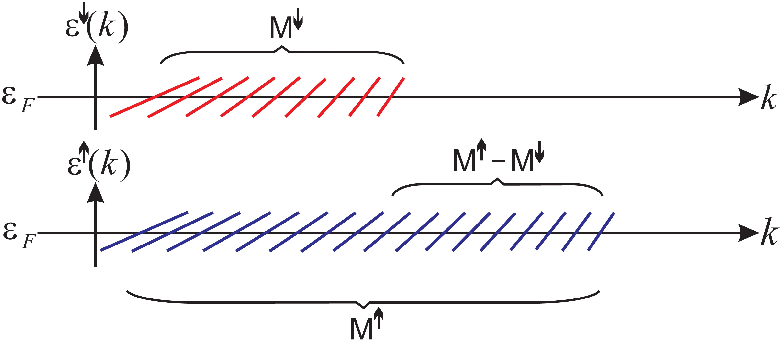
Figure 2. The dispersion curves around the Fermi energy for the different conductance channels. The bottom and top panels correspond to spin up and spin down electrons, respectively. Due to the exchange splitting the number of open conductance channels differs for the two spin subbands.
According to Eq. 2 the number of conductance channels can be formally written as:
Introducing a mean Fermi velocity, which is the average of the Fermi velocities for the different conductance channels weighted by the density of states of the channels,
and noting that is the total density of states at the Fermi level, the formula for the current spin polarization can be rewritten as:
This formula supplies a microscopic background for the conventional formulation of the current spin polarization [22], expressed by Fermi surface parameters of the two spin sub bands: density of states and Fermi velocity.
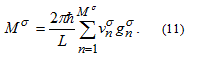
In real ferromagnets the exchange splitting of narrow d (or f) bands and the filling of the bands determine the magnetic properties (see Figure 5). The integral of the density of states up to the Fermi energy is different for the two spin orientations, which results in a finite magnetization, conventionally selecting the up spin as the majority spin orientation. However, the electron transport is determined by the Fermi surface properties. The spin polarized transport is not characterized by the magnetization, rather it is described by the spin polarization of the current, as described by Eq. 13. An interesting example is supplied by the Co or Ni type band fillings: the density of states at the Fermi level is much larger for the down spin, leading to a situation where the current spin polarization may take a sign opposite to that of the magnetization (Figure 5b).
Figure 5. Illustration of the density of states in ferromagnets. The magnetism is related to the exchange splitting of the narrow d (or f) bands. Panel (a) demonstrates the DOS in Fe: for minority spins (left side) the d band is above the Fermi level, whereas for majority spins (right side) the Fermi level lies inside the d band. Accordingly the DOS is significantly larger for the majority spins. Panel (b) demonstrates the DOS for Co and Ni type band filling. In this case is above the d band for majority spins, whereas it lies inside the d band for minority spins resulting in a negative Fermi surface spin polarization with respect to the positive magnetization.
Measurement of the current spin polarization and the spin diffusion length by superconducting Andreev spectroscopy
As shown in the previous section, there is an important difference between magnetization and current spin polarization. This difference highlights that magnetization measurements – for which various sensitive tools are available – are not an appropriate tool for the study of spin polarized transport. Somewhat closer information can be obtained by spin resolved photoemission spectroscopy, which measures the density of states spin polarization, 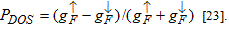 Nevertheless, for a close insight to the current spin polarization, direct transport measurements are necessary. There are several transport measurements revealing various consequences of spin polarized currents [24-28], but for a direct measurement of Pc only a few methods are available. In the following we demonstrate such a method based on point contact Andreev spectroscopy. (An alternative method is based on superconducting tunnelling spectroscopy in external magnetic field [29].)
The basic idea of Andreev spectroscopy is to measure the Andreev reflection of spin polarized conduction electrons on a superconductor surface [30-32]. When current is injected into the superconductor the charge must be converted to spin singlet Cooper pairs composed from two electrons with opposite spins. On the normal side an incoming electron drags an other electron with opposite spin and momentum, which is equivalent to reflecting a hole with opposite spin and momentum. This process is called Andreev reflection (Figure 6a). Compared to the single particle transfer (which occurs at voltages above the superconductor gap energy,  in the Andreev reflection double charge quanta are transmitted, and therefore the zero bias conductance may be even twice the high-bias, normal-state conductance. However, for a spin polarized metal the spin states available for the reflected hole are reduced (see Figure 6b), and the conductance is suppressed.
Figure 6. Panel (a): Illustration of Andreev reflection between a nonmagnetic metal and a superconductor. The incoming spin up electron is reflected as a spin down hole, and meanwhile a Cooper pair is created in the superconductor. Panel (b) demonstrates the absence of Andreev reflection between a fully spin polarized ferromagnet (half metal) and a superconductor. In this case no spin down states are available, and the Andreev reflection of the incoming spin up electrons is completely suppressed.
First we illustrate the consequences of Andreev reflection in a simple model geometry considering an ideal ferromagnetic quantum wire connected to a macroscopic superconducting electrode through an interface with perfect transmission. At a bias voltage much larger than the superconducting gap the superconducting features are not relevant, and the conductance of the device is dominated by the conductance of the quantum wire,
At zero bias this normal state conductance is strongly altered by Andreev reflections. An incoming electron can only be Andreev reflected if it has an opposite spin pair, i.e. all the minority spin channels  can be Andreev reflected to a majority spin state, but only
  majority spin channels can be Andreev reflected to a minority spin state. For these unpolarized channels the conductance doubles compared to the normal state conductance due to the transfer of double electron charge at each Andreev reflection process, i.e. the zero bias conductance can be written as:
from which a simple algebra yields a relation for the current spin polarization (see Eq. 5):
The above considerations show that the current spin polarization is simply determined by the ratio of the zero bias conductance and the normal state conductance of a point contact between a superconductor and the studied ferromagnetic metal. This picture, however, is only valid in an unrealistic model, where the ferromagnet-superconductor interface has perfect transmission, i.e. normal electron reflection is not considered at the interface. Considering a finite T transmission of the interface for a single channel nanowire the zero bias conductance is reduced compared to  even if the normal metal is not spin polarized
  . At zero temperature a zero bias conductance of
is obtained [10], yielding  in case of perfect transmissions, and a
  reduction for small transmission probabilities. Therefore, the ratio of the zero bias conductance and the normal state conductance is not enough information to tell whether an unpolarized metal with low transparency contact barrier or a highly spin polarized metal with transparent contact barrier is studied. However, the investigation of the entire nonlinear current voltage characteristic can make difference between these situations.
Different models have been developed to describe the shape of the current voltage characteristics of ferromagnet - superconductor nanojunctions as a function of the current spin polarization (Pc) and the transparency of the interface (T) [32-37]. In the most widely applied method the original Blonder-Tinkham-Klapwijk (BTK) theory of the Andreev reflection [38] is extended for ferromagnetic materials splitting the current to unpolarized and fully polarized parts, and then assuming no Andreev reflection for the fully polarized part and applying the BTK theory for the unpolarized part [33]. In an other, so-called Hamiltonian approach spin dependent transmission coefficients are considered, and their imbalance is deduced from the analysis of the  characteristics [32,34].
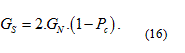
Figure 7 demonstrates  curves in limiting cases within the framework of the modified BTK theory: panel (a) shows an unpolarized contact with perfect and small transmission probabilities, wheres panel (b) demonstrates perfectly transparent contact with zero and perfect spin polarization. Whereas the zero bias conductance is heavily suppressed for both orange curves, the two cases yield a significantly different behaviour close to the gap: the high peak at
  in panel (a) is missing for highly spin polarized contacts (b) due to the absence of Andreev reflections. Due to this fundamental difference the fitting of experimental
  curves to the above finite temperature models can indeed yield both the transparency and the current spin polarization of the junction. The above idea was successfully used to get a direct experimental measure of the current spin polarization in various ferromagnetic metals [22,30-33,39-45] as well as more complex material systems [46], such as dilute magnetic semiconductors [47-49].
Figure 7. (a) Differential conductance curve of a normal metal superconductor junction calculated from the BTK theory [38] using zero temperature, zero spin polarization and (blue) and (orange). (b) Differential conductance curve calculated from the modified BTK theory [33] using zero temperature, perfect transmission and (blue) and (orange).
Experimentally the ferromagnet - superconductor interface is either created in an STM geometry by pushing a superconducting tip to a magnetic sample [30,33,40], or a nano-hole is fabricated in an isolating membrane, and afterwards the ferromagnetic and the superconducting layers are evaporated to the two sides of this hole [31,32,41].
To demonstrate the experimental determination of the current spin polarization Figure 8 shows the results of our study on a Nb-Fe nanojunction created in the tip - sample geometry. In panel (a) the experimental differential conductance curve is fitted by the modified BTK theory revealing a current spin polarization of . Pc = 0.62. This value is somewhat higher than the result of earlier studies [30,33], which may arise from the different surface preparation: in contrast to previous studies in our measurements a protective Au surface layer with a thickness of 5nm was applied to prevent the contamination of the Fe surface. The figure also demonstrates the accuracy of the method: if the spin polarization is fixed at a value slightly detuned from the optimal fit, no satisfactory fit is available by varying the barrier transparency (T). It is also found that the two theoretical models lead to essentially identical spin polarization values, even though they mathematically cannot be mapped onto each other.
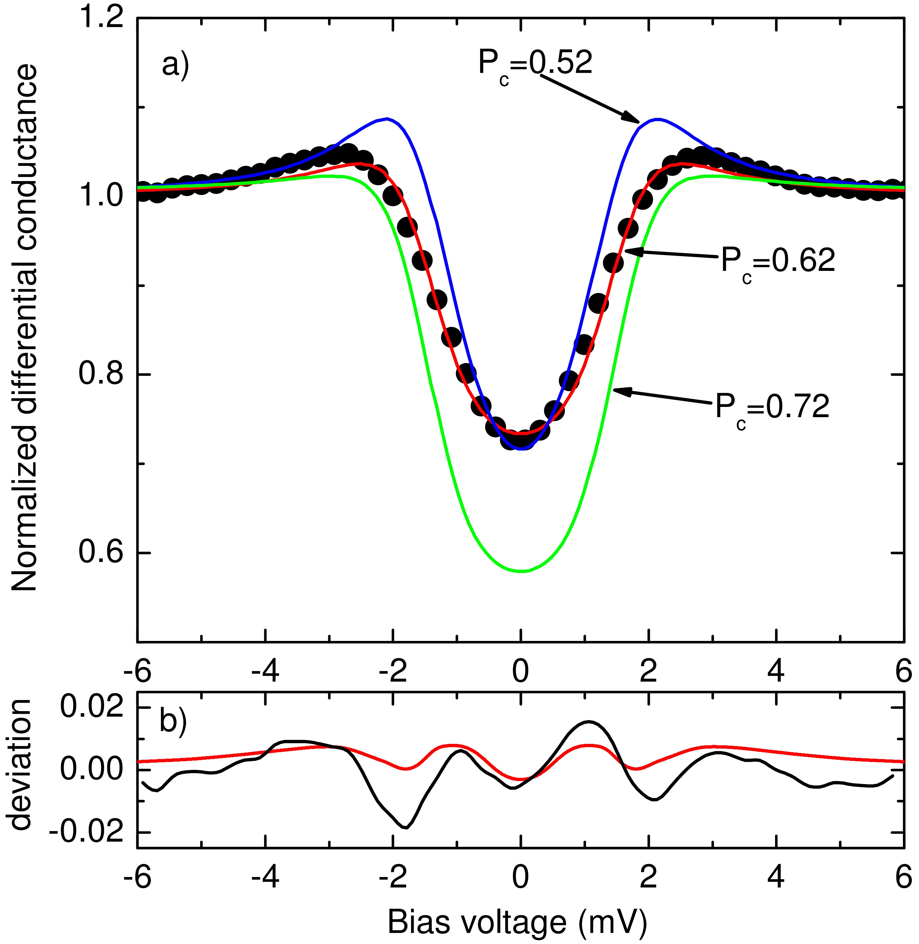
Figure 8. Panel (a) demonstrates the differential conductance curve measured between an Fe sample covered with 5nm Au capping layer and a Nb tip. The red line shows the best fit using the modified BTK theory, yielding a normal state resistance of  , a spin polarization of
  , a contact transparency of
  , a superconducting gap of
 at a temperature of 4.2 K. Note, that the normalized barrier strength, Z in the BTK theory is converted to transmission probability as
  . The blue and green lines show fits, where Pc is fixed at values intentionally detuned from the best fitting value, and only is used as a fitting parameter. These curves demonstrate that the resolution of the method is well below
  . Panel (b) demonstrates the deviation between the best fits based on the modified BTK theory and the Hamiltonian approach (red line). Although these two models do not give exactly the same fit, their deviation is smaller than the deviation of the experimental curve from the modified BTK fit (black line).
Another experimental example is presented in Figure 9a, demonstrating a differential conductance curve on Co-Nb junction. For cobalt the spin polarization is smaller than for iron: based on numerous measurements on various junctions  is obtained. This value agrees well with previous measurements performed on nano-hole samples [32].
It is worth noting, that the fitting functions contain two additional parameters: the temperature and the superconducting gap. We have found that for junctions in the ballistic limit the fitting results in a temperature which agrees well with the experimental temperature value. The gap also coincides with the bulk Nb gap, and the BCS temperature dependence of the gap [50] is clearly resolved by fitting the differential conductance curves of measurements at various temperatures (see Figure 9b). This consistency of the method is, however, lost if the contact size is increased and junctions in the diffusive limit are studied samples [48,51]. In this regime a considerable smearing of the curves is observed, and good fits are only possible if the fitting temperature is significantly larger than the experimental value. In extreme cases the fitting temperature may even grow above the critical temperature of Nb, which is an obvious contradiction.
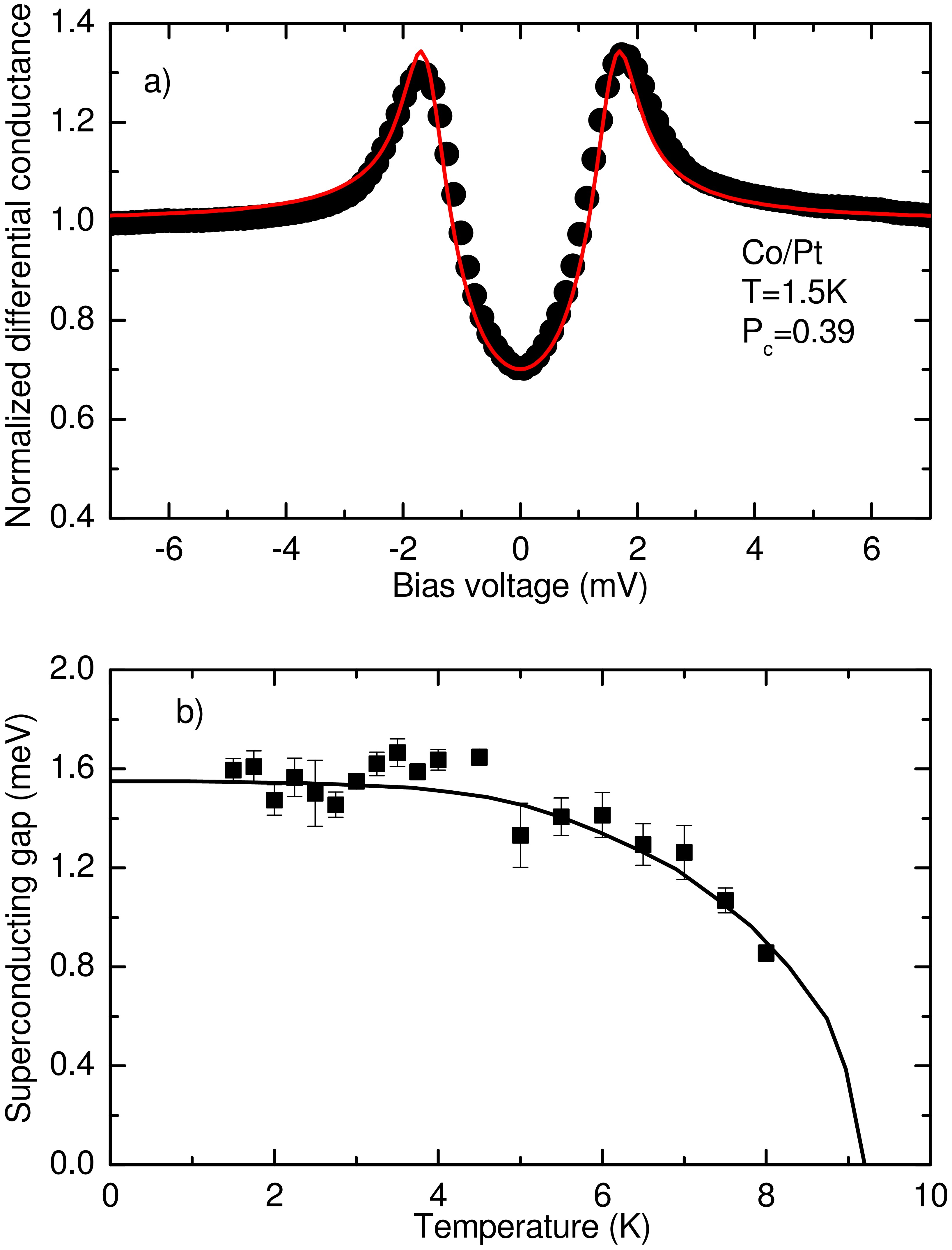
Figure 9. Panel (a) demonstrates the differential conductance curve for a nanojunction between a Nb tip and a Co sample with a Pt capping layer. The best fit (red line) yields  at a temperature of . Panel (b) demonstrates the temperature dependence of the fitted gap values clearly following the BCS prediction.
The above examples provide an insight to spin polarization measurement based on Andreev spectroscopy. This method provides a sensitive and reliable method for the direct determination of Pc if small ballistic junctions are used. For such junctions it is generally found that the results are not sensitive to the choice of the fitting model. However, for larger diffusive junctions the quality of the fits is significantly worse and accordingly the reliability of the method breaks down. Another requirement for the reliability of the method is the choice of a transparent junction. As Andreev reflection is a second order process, for low transparency junctions  its probability is suppressed and the differential conductance curve is not sensitive to the degree of spin polarization.
It is worth emphasizing that Andreev spectroscopy acts as a local probe technique, it is able to probe the spin polarization locally, at the nanometer scale [48]. In this sense it can be also applied to detect the lateral variations of the spin polarization.
In spintronic device applications not only the degree of the current spin polarization, but also its decay length in the nonmagnetic spacer layer is a property of utmost importance. For instance, as the separation of the magnetic layers in a GMR sensor becomes larger than the spin diffusion length the GMR effect exponentially decays [12,27].
Next we show that Andreev spectroscopy can also be used to determine spin diffusion length [52]. For this purpose a nonmagnetic capping layer is evaporated on the top of the ferromagnetic sample. The degree of spin polarization is measured at the surface of the capping layer, studying the decay of the spin polarization as the thickness of the capping layer is systematically increased. The carrier spin polarization is expected to decay exponentially as a function of the layer thickness. Figure 10 shows the results for Fe/Au samples clearly resolving this exponential decay, and yielding a spin diffusion length of  nm. This example further demonstrates that Andreev spectroscopy is a powerful tool to measure current spin polarization, and it may find even wider application as a local probe technique to study the lateral variation of at nanometer scale.
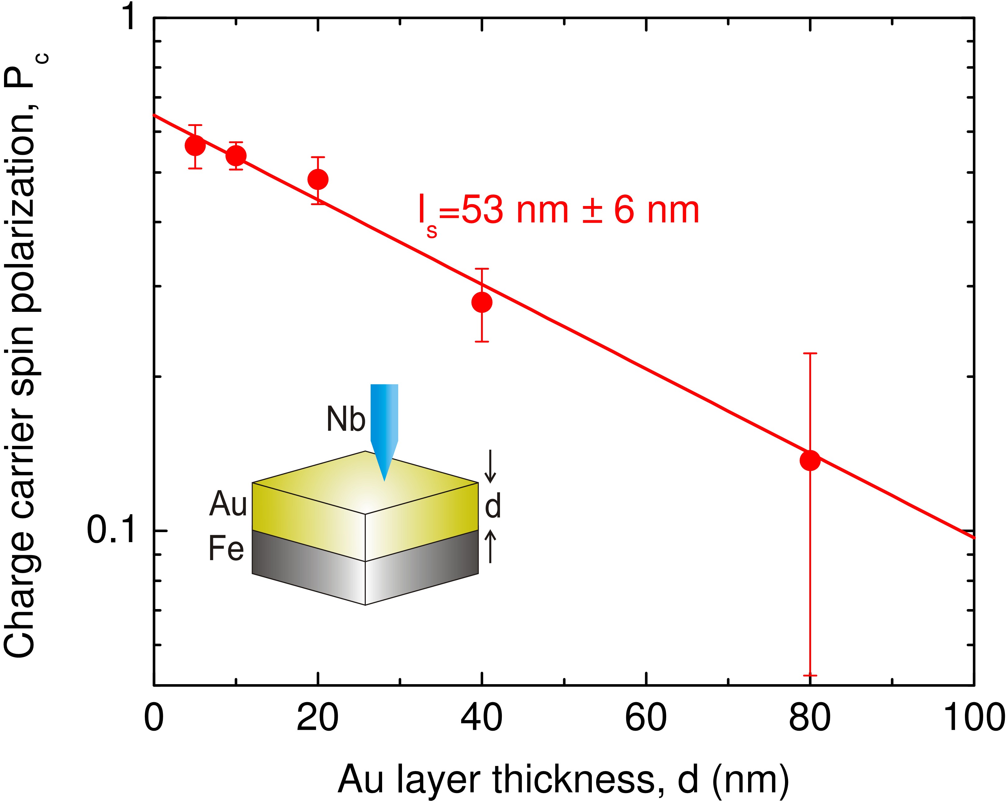
Figure 10. The measurement of spin diffusion length by Andreev spectroscopy. The inset demonstrates the experimental setup: on the top of Fe samples Au capping layers are evaporated with varying thickness. The current spin polarization is measured at the top of the Au layer as a function of the layer thickness. Each point in the figure corresponds to more than 10 independent junctions, which were created by lateral shifting the sample below the lifted Nb-tip by a piezo actuator. The error bars represent the scattering of the calculated polarization values for these independent experiments. The exponential decay of the spin polarization is clearly resolved as the Au layer thickness is increased yielding a spin diffusion length of  .
.
2021 Copyright OAT. All rights reserv
Nanoscale phenomena of spin related transport were discussed both theoretically and experimentally. Based on the spin dependent band structure of a magnetic metal, we reviewed the propagation of electrons in the ballistic and diffusive limits, and by applying the Landauer formalism, we supplied a nanoscopic background for the conventional expression of the current spin polarization. As the most direct experimental method for spin polarization measurements, the Andreev reflection spectroscopy was introduced, and experimental results on Fe and Co were shown. The analysis demonstrated the reliability of measurements carried out in the ballistic limit. The method was also extended for the determination of the spin diffusion length, one of the most important parameters of metals in spintronic applications.
This work was supported by the Hungarian research grant NKFI 112918.
Our experimental results demonstrating the method of superconducting Andreev spectroscopy were carried out in our custom-built system using a scanning tunnelling microscope geometry. Mechanically sharpened Nb tips were used as the superconductor counter-electrode gently touching the top of the metallic layer. High stability point contacts were created using a screw mechanism and a three-dimensional piezo actuator for fine tuning. To check the scattering of the data measurements were carried out at several different positions on the samples. The temperature dependent measurements were performed in a variable temperature liquid helium cryostat.
- Wolf SA, Awschalom DD, Buhrman RA, Daughton JM, von Molnar S, et al. (2001) Spintronics: A Spin-Based Electronics Vision for the Future. Science 294: 1488. [Crossref]
- Awschalom DD, Flatte ME (2007) Spintronics: Challenges for semiconductor spintronics. Nat Phys 3: 153.
- Han W, Kawakami RK, Gmitra M, Fabian J (2014) Graphene spintronics. Nat Nano 9: 794. [Crossref]
- Dietl T, Ohno H (2014) Dilute ferromagnetic semiconductors: Physics and spintronic structures. Rev Mod Phys 86: 187.
- Jedema FJ, Filip AT, van Wees BJ (2001) Electrical spin injection and accumulation at room temperature in an all-metal mesoscopic spin valve. Nature 410: 345. [Crossref]
- Linder J, Robinson JWA (2015) Superconducting spintronics. Nat Phys 11: 307.
- Zutic I, Fabian J, Das Sarma S (2004) Spintronics: Fundamentals and applications. Rev Mod Phys 76: 323.
- Gregg JF, Petej I, Jouguelet E, Dennis C (2002) Spin electronics - a review. Journal of Physics D: Applied Physics 35: R121.
- Landauer R (1981) Can a length of perfect conductor have a resistance? Physics Letters A 85: 91.
- Nazarov YV, Blanter YM (2009) Quantum Transport (Cambridge University Press).
- Datta S (1995) Electronic transport in mesoscopic systems (Cambridge University Press).
- Valet T, Fert A (1993) Theory of the perpendicular magnetoresistance in magnetic multilayers. Phys Rev B 48: 7099. [Crossref]
- Agrait N, Yeyati AL, van Ruitenbeek JM (2003) Quantum properties of atomic-sized conductors. Physics Reports 377: 81.
- van Wees BJ, van Houten H, Beenakker CWJ, Williamson JG, Kouwenhoven LP, et al. (1988) Quantized conductance of point contacts in a two-dimensional electron gas. Phys Rev Lett 60: 848. [Crossref]
- Ihn T (2010) Semiconductor Nanostructures (Oxford UniversityPress).
- Buttiker M, Imry Y, Landauer R, Pinhas S (1985) Generalized many-channel conductance formula with application to small rings. Phys Rev B 31: 6207. [Crossref]
- Baibich MN, Broto JM, Fert A, Van Dau FN, Petro P (1988) Giant Magnetoresistance of (001)Fe/(001)Cr Magnetic Superlattices. Phys Rev Lett. 61: 2472. [Crossref]
- Binasch G, Grunberg P, Saurenbach F, Zinn W (1989) Enhanced magnetoresistance in layered magnetic structures with antiferromagnetic interlayer exchange. Phys Rev B 39: 4828.
- Hafner M, Viljas JK, Frustaglia D, Pauly F, Dreher M, et al. (2008) Theoretical study of the conductance of ferromagnetic atomic-sized contacts. Phys Rev B 77:104409.
- Vardimon R, Klionsky M, and Tal O (2015) Indication of Complete Spin Filtering in Atomic-Scale Nickel Oxide. Nano Letters 15: 3894. [Crossref]
- Beenakker CWJ (1997) Random-matrix theory of quantum transport. Rev Mod Phys 69: 731.
- Woods GT, Soulen RJ, Mazin I, Nadgorny B, Osofsky MS, et al. (2004) Analysis of point-contact Andreev reflection spectra in spin polarization measurements. Phys Rev B 70: 054416.
- Raue R, Hopster H, Clauberg R (1983) Observation of Spin-Split Electronic States in Solids by Energy-, Angle-, and Spin-Resolved Photoemission. Phys Rev Lett. 50: 1623.
- Datta S, Das B (1990) Electronic analog of the electro‐optic modulator. Applied Physics Letters 56: 665.
- Ohno Y, Young DK, Beschoten B, Matsukura F, Ohno H, et al. (1999) Electrical spin injection in a ferromagnetic semiconductor heterostructure. Nature 402: 790.
- Hammar PR, Bennett BR, Yang MJ, Johnson M (1999) Observation of Spin Injection at a Ferromagnet-Semiconductor Interface. Phys Rev Lett 83: 203.
- Bass J, Pratt WP (2007) Spin-diffusion lengths in metals and alloys, and spin-flipping at metal/metal interfaces: an experimentalist's critical review. Journal of Physics: Condensed Matter 19: 183201.
- Valenzuela SO, Tinkham M (2006) Direct electronic measurement of the spin Hall effect. Nature 442: 176. [Crossref]
- Tedrow PM, Meservey R (1971) Spin-Dependent Tunneling into Ferromagnetic Nickel. Phys Rev Lett 26: 192.
- Soulen RJ, Byers JM, Osofsky MS, Nadgorny B, Ambrose T, et al. (1998) Measuring the spin polarization of a metal with a superconducting point contact. Science 282: 85. [Crossref]
- Upadhyay SK, Palanisami A, Louie RN, Buhrman RN (1998) Probing Ferromagnets with Andreev Reflection. Phys Rev Lett 81: 3247.
- Perez-Willard F, Cuevas JC, Surgers C, Pfundstein P, Kopu J, et al. (2004) Determining the current polarization in Al/Co nanostructured point contacts. Phys Rev 69: 140502.
- Strijkers GJ, Ji Y, Yang FY, Chien CL, Byers BL (2001) Andreev reflections at metal/superconductor point contacts: Measurement and analysis. Phys Rev B 63: 104510.
- Cuevas JC, Martin-Rodero A, Yeyati AL (1996) Hamiltonian approach to the transport properties of superconducting quantum point contacts. Phys Rev B 54: 7366. [Crossref]
- Nurbawono A, Zhang C (2012) Sensing with Superconducting Point Contacts. Sensors 12: 6049. [Crossref]
- Grein R, Lofwander T, Metalidis G, Eschrig M(2010) Theory of superconductor-ferromagnet point-contact spectra: The case of strong spin polarization. Phys Rev B 81: 094508. [Crossref]
- Cottet A, Belzig W (2008) Conductance and current noise of a superconductor/ferromagnet quantum point contact. Phys Rev B 77: 064517.
- Blonder GE, Tinkham M, Klapwijk TM (1982) Transition from metallic to tunneling regimes in superconducting microconstrictions: Excess current, charge imbalance, and supercurrent conversion. Phys Rev B 25: 4515.
- Ji Y, Strijkers GJ, Yang FY, Chien CL, Byers JM, et al. (2001) Determination of the Spin Polarization of Half-Metallic CrO2 by Point Contact Andreev Reflection. Phys Rev Lett. 86: 5585. [Crossref]
- Kant CH, Kurnosikov O, Filip AT, LeClair P, Swagten HJM, et al. (2002) Origin of spin-polarization decay in point-contact Andreev reflection. Phys Rev B 66: 212403.
- Stokmaier M, Goll G, Weissenberger D, Surgers C, Lohneysen HV (2008) Size Dependence of Current Spin Polarization through Superconductor/Ferromagnet Nanocontacts. Phys Rev Lett. 101: 147005. [Crossref]
- Lofwander T, Grein R, Eschrig M (2010) Is CrO2 Fully Spin Polarized? Analysis of Andreev Spectra and Excess Current. Phys Rev Lett 105: 207001. [Crossref]
- Rajanikanth R, Kasai S, Ohshima N, Hono K (2010) Spin polarization of currents in Co/Pt multilayer and Co–Pt alloy thin films. Applied Physics Letters 97: 022505.
- Gramich J, Brenner P, Surgers C, Lohneysen HV, Goll G (2012) Experimental verification of contact-size estimates in point-contact spectroscopy on superconductor/ferromagnet heterocontacts. Phys Rev B 86: 155402.
- Loehneysen H, Beckmann D, Goll G, Willard FP, Stalzer H, et al. (2007) Proximity effect between superconductors and ferromagnets. Physica C: Superconductivity and its Applications Part 1: 322.
- Krivoruchko VN, D'yachenko AI, Tarenkov VY (2013) Point-contact Andreev-reflection spectroscopy of doped manganites: Charge carrier spin-polarization and proximity effects. Low Temperature Physics 39: 211.
- Braden JG, Parker JS, Xiong P, Chun SH, Samarth N (2003) Direct Measurement of the Spin Polarization of the Magnetic Semiconductor (Ga,Mn)As Phys Rev Lett. 91: 056602. [Crossref]
- Geresdi A, Halbritter A, Csontos M, Csonka S, Mihaly GT, et al. (2008) Nanoscale spin polarization in the dilute magnetic semiconductor (In, Mn) Sb Phys Rev B 77: 233304.
- Akazaki T, Yokoyama T, Tanaka Y, Munekata H, Takayanagi H (2011) Evaluation of spin polarization in p-In0.96Mn0.04As using Andreev reflection spectroscopy including inverse proximity effect. Phys Rev B 83: 155212
- Townsend P, Sutton J (1962) Investigation by Electron Tunneling of the Superconducting Energy Gaps in Nb, Ta, Sn, and Pb. Phys Rev 128: 591.
- Chalsani P, Upadhyay SK, Ozatay O, Buhrman RA (2007) Andreev reflection measurements of spin polarization. Phys Rev B 75: 094417.
- Geresdi A, Halbritter A, Tancziko F, Mihaly G (2011) Direct measurement of the spin diffusion length by Andreev spectroscopy. Applied Physics Letters 98: 212507.