Abstract
Atomically precise thin-film deposition techniques have innovated material synthesis, leading to supperlattices and nanolaminates, and yet we face a further challenge to synthesize atomically precise complex structures like atomically precise dot superlattices. Herein, we hypothesize an integrated system of atomic layer deposition and atomically precise dot deposition. Atomic layer deposition exploits a vacuum process to quickly switch at least two reactants in a stepwise manner. By contrast, atomically precise dot deposition necessitates a wet process because high molecular-weight dot precursors specify the number of metal ions to form the dots. As the first step to integrate the vacuum process and the wet process into a total system, we demonstrated a uniform wide-angle spray to control the amount of dot precursors on substrate in a vacuum chamber with one shot. We also suggest the expected benefits and the applications including electronic battery to encourage the further system developments. Since we expand the logic of chemical synthesis in organic chemistry into inorganic synthesis, inorganic materials can obtain a wide variety of atomically precise complex structures that organic materials and biological systems possess.
Keywords
atomically precise architectonics, logic of chemical synthesis, complex system, solvation
Introduction
Materials science has fully developed, allowing us to predict almost full of material properties with a high accuracy using the first principal calculation based on the band theory. In other words, atomic properties decide the bond lengths, the crystal structures, and the band structures, and then fate the material properties [1]. As material properties, we found superconductivity one century ago. Superconductivity would reduce the transmission energy loss during the energy supply from power plants. We also found Seebeck effect for thermoelectrics two centuries ago. Thermoelectrics can recover electricity from waste heat produced by necessity when we use energy. Since these functionalities are expected to dramatically change the energy usage and our life style, researchers have strived to develop high temperature superconductors and thermoelectric materials efficiently generating electricity from small temperature differences. Still, these achievements do not fully meet the demands for the wide distributions to the human society over the centuries. To overcome the difficulties in the current materials science, we need the alternative radical ways to cultivate an untrodden materials science, for example, using a high pressure to change the bond lengths and the atomic arrangements [2].
As another innovative concept, we acknowledge superlattice and nanolamination fabricated with atomically precise thin-film deposition techniques: physically, molecular beam epitaxy (MBE) [3]; and chemically, atomic layer deposition (ALD) [4], where the properties depend on the compositions and the thicknesses. These nanostructures have attracted huge attention because atomically layered copper oxides transit to the superconducting phase at high temperature over the boiling point of liquid nitrogen [5]. In relation to atomically precise complex structures, we can observe emergent functions in biological systems, such as light harvesting, photosynthesis, and biocatalysts, where functional molecular moieties are three-dimensionally arranged with atomic precision. These moieties interact each other and cooperatively perform the emergent functions free from atomic properties. Artificially, multistep organic synthesis can prepare molecular systems mimicking some of biological emergent functions via atomically restricting
chemical reaction points to obtain complex molecular structures with atomic precision [6]. In a case of dendrimers, for example, we synthesize perfectly brunched molecular trees based on divergent or convergent methods in stepwise manners [7]. Consequently, we can design the three-dimensional position of functional molecular moieties on the core, the brunches, and the terminals to demonstrate biological emergent functions [8]. Another good example of emergent properties is photovoltaic property of dye-sensitized solar cells [9]. Although the individual components do not have any photovoltaic property, dye-sensitized solar cells present emergent photovoltaics as a whole. It suggests that dreamlike properties may emerge from well-known material components. In short, atomically precise complex structures are the key to create a materials science free from atomic properties.
Herein, we can find a similarity between multistep organic synthesis and ALD. In an ideal ALD cycle, ALD precursors are chemically adsorbed on surfaces with a self-limiting manner, and then chemically transformed with into the single-monolayer thin films [10, 11]. Therefore, the cycle number controls the film thickness with atomic precision. In the multistep process, the self-limiting manner of ALD precursors atomically defines the number of metal ions as the chemical reaction points, identically with multistep organic synthesis. In fact, we can expand the logic of chemical synthesis to atomically precise dot deposition (APD2). We simply prepare the single or less molecular layer of dot precursors defining the number of metal ions for reactions inside the dot precursors, and then chemically convert the dot precursors into atomically precise dots. In the case of TiO2, we have confirmed the size dependences in the bandgap of the anatase and the rutite structures, suggesting no large-size contaminants exist [12].
We have also confirmed the size dependences in the anatase-rutie phase transition initiation temperature, suggesting no small-size contaminants exist [13]. Overall, the concept of APD2 has been already demonstrated [14]. Note that people cannot control dot structures with atomic precision based on physical method MBE because MBE generates dot structures from strain between the first and the second deposited layers using lattice mismatch [15]. Similarly, metal thin films prepared by ALD and sputter deposition also give small dots during the nucleation process, especially when adhesion between metal and substrate is poor. However, these small dots never acquire atomic precision because the random occurrence of the nucleation process causes the statistical distribution in the dot structures [16, 17]. In principal, the conventional thin-film deposition techniques do not involve any procedures to control dot structures with atomic precision. Based on the logic of chemical synthesis, the combination of ALD and
APD2 creates a wide variety of atomically precise complex structures with inorganic materials: namely, multistep inorganic synthesis of thin films (Figure 1).
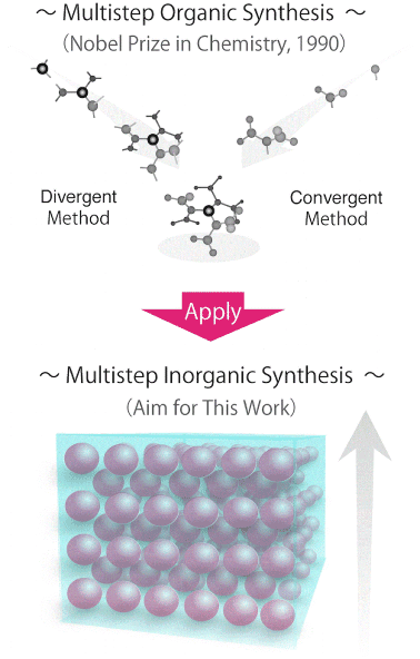
Figure 1. Concept of this work, applying the logic of chemical synthesis in organic chemistry to inorganic synthesis
From a technical viewpoint of thin-film deposition, we prefer automatizing the combinational scheme. For this purpose, however, we must integrate the vacuum process and the wet process. ALD matches a vacuum process because we need to switch A and B reactants for the atomically precise fabrication. Simple gas exchanging is much faster and more efficient than liquid exchanging or changing reactant solutions for dipping substrates [14]. In contrast, APD2 necessitates a wet process because we cannot vaporize high molecular weight dot precursors consisting multiple metal ions and spacing ligands. Furthermore, we need to regulate the amount of dot precursors on substrate to form the single or less molecular layers. In a drop cast process, the concentration and the volume of dot-precursor solutions determine the amount [12-14]. Otherwise, the dots aggregate to lost the atomic precision after the chemical conversion of dot precursors. The easiest way to combine these processes is to connect the vacuum process chamber and the wet process chamber through a substrate transfer system, but inefficient as a deposition process. Thus, we consider employing a spray technique to spread solution of the dot precursors into an ALD vacuum chamber (Figure 2). In this case, we can expect to shorten the total deposition time by 1/20. The spray technique, however, should spread the solution uniformly over a large area so that the dot precursors can form the single or less molecular layers by tuning the spray time and the concentration. In the major spray types: one-fluid type and two-fluid type, one-fluid type spray can spread solution uniformly over a large area under the ambient condition when we chose appropriate full cone spray nozzles. Inside of the one-fluid nozzle, liquid fluid whirls to shoot out from the outlet with a wide angle 60º-90º and a uniform-shape distribution. Under a vacuum condition, however, one-fluid type spray causes dripping because vacuum pulls out liquid remained between the nozzle and a valve. Contrastively, two-fluid type spray does not cause dripping because a needle seals up the outlet to control the flow of liquids, yet liquids mixed with atomizing gas shoots out straightly with a small angle 5º- 10º and a mountain-shape distribution. In this paper, therefore, we report a new spray design to deliver uniform and wide angle spray patterns with one shoot under a vacuum condition. We also discuss the expected benefits and the applications of the ALD-APD2 integrated system to encourage the further system developments.

Figure 2. Schematic process of the ALD-APD2 integrated system
Results and Discussion
To achieve uniform and wide-angle spray patterns under a vacuum condition, we adjusted the fluid control manner in two-fluid type spray to one-fluid type spray. We cannot simply seal up the outlet of one-fluid nozzle with a needle because whirling liquid fluid inside the nozzle is the key process to achieve a uniform and wide-angle spray. If a needle seals up the outlet of one-fluid nozzle, liquid initially filled inside the nozzle does not gain enough whirling to shoot out with a wide angle when the needle opens the outlet. The volume inside the nozzle may be small, but it can considerably lower the quality because the volume is comparable to the spray amount to obtain the single or less molecular layers. Thus, we use a rod instead of the needle to seal up all the inlets of a one-fluid nozzle because the one-fluid nozzle we choose has four inlets to start whirling liquid fluid directly from the positions (Figure 3a). As the first test, we confirmed a uniform spray pattern of water on Kimtowel under 100 Torr without dripping.
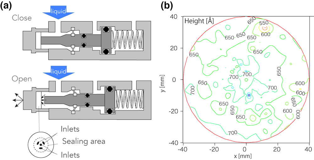
Figure 3. Design of uniform wide-angle spray unit (a), and height mapping image of polyvinyl acetate film sprayed from the mix solvent of toluene and chlorobenzene (v/v = 1/1) (b).
Secondly, we tested the newly designed spray unit for forming films on glass substrates from solutions of polyvinyl acetate, using a scanning ellipsometry. We found that the mix solvent of toluene and chlorobenzene (v/v = 1/1) films more uniformly than toluene- or chlorobenzene-only solvents (Figure 3b). Toluene and chlorobenzene contribute to a good spread and a nice drying process, respectively. Both of the processes critically affect the uniformity of films. The result suggests that we need to choose solvents, mixture ratios, and additives depending on ALD chamber conditions. We also observed the thickness fairly matching with the calculated one from the spray conditions, such as spray angle φ, flow rate F, distance between spray unit and substrate D, spray time t, and solution concentration M. Based on the results, we can estimate the spray conditions to prepare a fully packed single-molecular layers as the maxim spray amount: for example, D = 10 cm, t = 0.2 s, and M = 1.8 × 10⁵ mol/l for the same spray nozzle with φ = 60º and F = 0.5 l/min. under an assumption of a spherical dot precursor with 2 nm in diameter. Thus, we conclude that the newly designed spray unit overcomes the first obstacle to automatize the combinational scheme.
To complete the simple concept of integrating ALD and APD2 processes as a total system, we actually need to control each of the processes complexly (Figure 4). Although the ALD process switches the reactant gases inside the reaction chamber, the simple process conformally deposits the films anywhere the reactant gases diffuse into and normally necessitates heat to activate the surface chemical reactions and to avoid condensing ALD precursor gases into the liquids or solids inside the reaction chamber. Therefore, we first have to insert a gate valve between the spray unit and ALD chamber to protect the spray unit against film deposition and heat from the reaction chamber. Secondly, we need to stop the flow and the exhaust of carrier gases during the spray not to disrupt the spray patterns. Thirdly, a heater can control temperature of the sample holder independently from another heater for the reaction chamber to directly supply enthalpy of vaporization for the sprayed solution on the sample substrates. Furthermore, we can nominate to cap the sealing rod with a chemically resistive soft cushion to improve the sealing and the durability. From a reliability viewpoint, the soft cushion would reduce the mechanical damage on the spray nozzle cased by the sealing rod. Again, to achieve uniform spray patterns through the drying process, we can choice or mix high-boiling-point solvents, for example, solvents used in direct-liquidinjection/evaporation chemical vapor deposition [18] and set temperatures of the chamber and the sample holder lower than the boiling points. Finally, to recover a vacuum condition for the subsequent ALD process after the APD2 process, we can trap the vaporized solvents with a cold trap at the downstream before the vacuum pump. As an additional task especially for atomically precise control of dot superlattices, we need to design intermolecular interactions of the dot precursors and maybe arraying additives to assist the supermolecular assembly of dot precursors as a template for dot array layers via the simple one short spray. Overall, we still have many tasks to automatize the advanced atomically precise fabrication system.
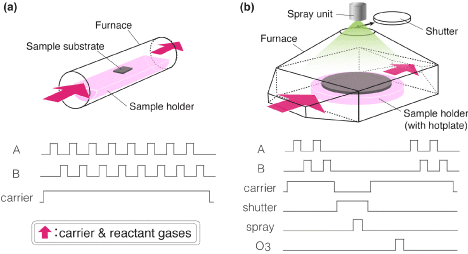
Figure 4. Comparisons between ALD system (a) and ALD-APD2 integrated system (b) in reactor design and sequence
To justify performing these tasks, we discuss differences that the integrated fabrication system would make. Compared with quantum dots prepared with MBE: typically cones with 10 ~ 20 nm in diameter and 2 ~ 5 nm in height, APD2 can fabricate molecular-scale dots with less than 2 nm in diameter and 10-100 times higher dot density. Assuming dots embedded in media having finite energy barrier, we can expect that much more electron of APD2 dots penetrates into the surrounding media than that of MBE dots. Under the high dot density condition, the penetrated electrons could correlate each other between APD2 dots towards emergent electromagnetic functions. In addition to the correlation between APD2 dots, we must emphasize correlation between APD2 dots and the surrounding media. Due to the molecularity, we can assume that the APD2 dots are solvated by the ALD surrounding media [19]. Since electron of the molecular-scale dots penetrates into the ALD surrounding media much more than that of MBE dots, the height of energy barrier drastically changes electromagnetic properties of the dots. It equals molecular system where molecules show totally different electromagnetic properties and chemical reactivity in different solvents.
In connection with the importance of solvation, we expect the difference in electric conductance between the atomically precise dot material system and organic semiconductors including molecular crystals and polymer films [20, 21]. In these molecular systems, electric conductance can be explained by Marcus theory as molecular-scale electron transfer where dynamics of the surrounding media including solvents dominates the electron transfer via activating molecules to the transition states [22]. From a viewpoint of solvation, the conductive organic molecules/polymers are solvated by the surrounding molecules/polymers themselves. The dielectric constants are generally low, which is not beneficial to stabilize charge localized on the molecules/polymers and assist the charge transports [19]. By contrast, the atomically precise dot material system can design the charging sites and the surrounding media independently based on the combination of ALD and APD2. Molecular-scale electron transfer is also one of emergent functions after all. In short, the ALD-APD2 integrated system would create the atomically precise dot material system with large capabilities to design emergent functions.
Overviewing electron manipulation technology, we additionally clarify novelty of the atomically precise dot material system. In the current electronics, we use semiconductors where electron obeys a Boltzmann distribution. The distribution has limited efficient transition in conductivity. Although quantum dots have quantized energy levels with no distribution [23], less than 2-nm dots are necessitated to maintain the energy levels over room temperature so that electric charging energy can overcome thermal energy at room temperature [24]. To suppress the manufacturing distribution in the dot size and properties less than 10 %, we need to fabricate the dots with atomic precision. To avoid the difficulty, single atoms and molecules have been nominated as the quantum dots [25, 26]. Yet, the atomically precise structure cannot maintain over room temperature because single atoms and molecules freely diffuse on surface to survey the stable binding sites. More importantly, solvation has been ignored. In molecular scale, again, dynamic of surrounding solvents dominates electron transfer, as explained by Marcus theory [19, 22]. By contrast, electrochemical devices like lithium ion battery successfully benefit from solvation to manipulate electrons on ions over room temperature. In these devices, however, ion transports and exchange reactions determine the rate of responses and mechanical durability of electrodes [27]. In short, electrochemical devices manipulate electrons over room temperature but not purely. Herein, we can recognize the atomically precise dot material system as APD2 dots solvated by ALD media to provide avant-garde pure electron manipulation on quantized energy levels with solvation over room temperature (Table 1).
Table 1. Comparison in electron manipulation technologies
|
|
Electronics |
|
Electrochemistry |
|
Atomically precise dot material system |
Semiconductor |
Quantum dot |
In solution/Solid state ionics |
|
Temperature |
|
Room temperature |
Cryogenic |
|
Room temperature |
|
Room temperature |
Size |
|
Bulk |
100 nm to atom/molecule |
|
Atom/molecule |
|
Molecular sale |
Electric state |
|
Boltzmann distribution |
Quantized |
|
Quantized |
|
Quantized |
Solvation |
|
None |
Ignorable/disregarded |
|
Utilized |
|
Utilized |
Solvent |
|
None |
None |
|
Utilized/none |
|
None |
Rate-determining step |
|
Electron diffusion |
Electron tunneling |
|
Ion transport & exchange reaction |
|
Electron transfer |
Based on the distinguishable characteristics, we have suggested some applications. As an application, we can expect single-electron electronics using the solvated quantized energy levels known as redox potentials [19]. Considering the current interests in two-dimensional electronics [28], we also regard the atomically precise dot array as an artificial two-dimensional material with tunable artificial atomic sizes, bonding lengths, and packing structures to expand a variety of two-dimensional electronics. From an aspect of the structural periodicity matching with phonon wavelength over room temperature, we assume the atomically precise dot material system as an ideal phononic crystal [29]. Thus, the atomically precise dot material system has a potential of low thermal conductivity. The combination with electric conduction discussed above may lead to high performance thermoelectric materials. In addition to the thermoelectric application, we can expect unique phononic applications like phononic diode [30]. Overall, the atomically precise dot material system would impact on wide research areas.
As a contribution to energy storage, we also propose a concept of electric battery based on the atomically precise dot material system. Historically, humans have developed capacitor, rechargeable battery, and electrochemical capacitor in the 18th, 19th and 20th centuries, respectively. Capacitors use dielectric materials to store electrical energy. In an ideal condition: zero dielectric loss, electron simply transfers through external circuit. Thus, capacitors basically show quick response and long durability. On the other hand, electrochemical reactions of electrode materials play a key role in rechargeable batteries, advantaging energy density [27]. During the operation, rechargeable batteries show plateau in voltage based on two redox potentials of electrode materials. As mentioned above, however, ion transports and exchange reactions determine the rate of charge/discharge. Especially, quick charge/discharge provokes undesired reactions to mechanically damages the electrode materials and create excess heat as a cause of thermal runaway and fire. In contrast, electrochemical capacitors mainly use ion adsorptions on nanostructured electrodes [31]. Similar to rechargeable batteries, the ion transports basically determine the rate of charge/discharge. The physical ion adsorptions, however, less damage the electrode materials than the ion exchange reactions in rechargeable batteries. Electrochemical capacitors have the middle performances between capacitors and rechargeable batteries. Herein, we can classify these energy storage technologies into four quadrants according to whether physical storage or chemical storage and whether electron-driven or ion-driven: capacitors [physical storage & electron-driven], rechargeable batteries [chemical storage & ion-driven], and electrochemical capacitors [physical storage & ion-driven] (Figure 5). Then, we can find a new possibility in the quadrant [chemical storage & electron driven], requiring redox reactions without ion transports and exchange reactions. This is exactly what the atomically precise dot material system can offer, namely electric battery.
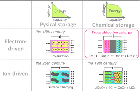
Figure 5. Quadrant analysis of energy storage technologies
Conclusions
Hypothesizing the ALD-APD2 integrated system based on the logic of chemical synthesis; we have demonstrated uniform wide-angle spray under a vacuum condition as the first paving stone to automatize multistep inorganic synthesis of thin films. Although we still have many tasks to establish the ALD-APD2 integrated system, we have enough reasons to perform these tasks. We expect the atomically precise dot material system to cultivate an untrodden materials science of inorganic emergent functions and the distinguishable applications. The ALD-APD2 integrated system would assist to survey the full potential of the atomically precise dot material system derived from innumerable structural potential: the dot size, the ALD thickness, the compositions, and the hierarchical homo/hetero superstructures.
Methods
All the chemicals were purchased from Kantoh Kagaku. Polyvinyl acetate was prepared to be 2.5 g/l with toluene and chlorobenzene (v/v = 1/1). The spray unit was prepared by modifying Super-Small, Constant-Volume Dispensing Valve (NCV-17, Musashi Engineering Inc.) to attach Small Capacity Full Cone Spray Nozzles (1/8M JJRP 005 PTFE, H. IKEUCHI & Co., Ltd.). Digital control valve controller (VALVE MASTER ME-5000VT, Musashi Engineering Inc.) controlled the spray pressure and spray time to be 0.2 MPa and 0.2 s, respectively. The scanning ellipsometry was performed with Automatic Laser Ellipsometer (MARY-102FM, Five Lab Co., Ltd.).
Acknowledgements
The author thanks N. Shibazaki and M. Nakao for their useful discussions, H. IKEUCHI & Co., Ltd. And Musashi Engineering Inc. for their material and technical supports, and T. Kimura for his technical assistances. This work is practically supported by JSPS KAKENHI Grant Number 15H05406.
References
- Langmuir I (1919) The arrangement of electrons in atoms and molecules. J Am Chem Soc 41: 868-934.
- Drozdov AP, Eremets MI, Troyan IA, Ksenofontov V, Shylin SI (2015) Conventional superconductivity at 203 kelvin at high pressures in the sulfur hydride system. Nature 525: 73-76. [Crossref]
- Cho AY, Arthur JR (1975) Molecular beam epitaxy. Prog Solid State Chem 10: 157-192.
- Puurunen RL (2014) A Short history of atomic layer deposition: Tuomo Suntola's atomic layer epitaxy. Chem Vap Deposition 20: 332-344.
- Keimer B, Kivelson SA, Norman MR, Uchida S, Zaanen J (2015) From quantum matter to high temperature superconductivity in copper oxides. Nature 518: 179-186. [Crossref]
- Corey EJ (1991) The logic of chemical synthesis: Multistep synthesis of complex carbogenic molecules (Nobel Lecture). Angew Chem Int Ed 30: 455-465.
- Tomalia DA, Fréchet JMJ (2002) Discovery of dendrimers and dendritic polymers: A brief historical perspective. J Polym Sci Part A: Polym Chem 40: 2719-2728.
- Astruc D, Boisselier E, Ornelas C (2010) Dendrimers designed for functions: from physical, photophysical, and supramolecular properties to applications in sensing, catalysis, molecular electronics, photonics, and nanomedicine. Chem Rev 110: 1857-1959. [Crossref]
- Satoh N, Han L (2012) Chemical input and I-V output: stepwise chemical information processing in dye-sensitized solar cells. Phys Chem Chem Phys 14: 16014-16022. [Crossref]
- Leskelä M, Ritala M (2003) Atomic layer deposition chemistry: recent developments and future challenges. Angew Chem Int Ed Engl 42: 5548-5554. [Crossref]
- George SM (2010) Atomic layer deposition: an overview. Chem Rev 110: 111-131. [Crossref]
- Satoh N, Nakashima T, Kamikura K, Yamamoto K (2008) Quantum size effect in TiO2 nanoparticles prepared by finely controlled metal assembly on dendrimer templates. Nat Nanotechnol 3: 106-111. [Crossref]
- Satoh N, Nakashima T, Yamamoto K (2013) Metastability of anatase: size dependent and irreversible anatase-rutile phase transition in atomic-level precise titania. Sci Rep 3: 1959. [Crossref]
- Satoh N (2015) Soft matter assembly for atomically precise fabrication of solid oxide. In: Chen X, Fuchs H eds. (2015) Soft Matter Nanotechnology. Weinhein: Wiley-VCH. Ch. 8: 217-232.
2021 Copyright OAT. All rights reserv
- Shchukin VA, Dieter B (1999) Spontaneous ordering of nanostructures on crystal surfaces. Rev Mod Phys 71: 1125-1171.
- Lu J, Low KB, Lei Y, Libera JA, Nicholls A, et al. (2014) Toward atomically-precise synthesis of supported bimetallic nanoparticles using atomic layer deposition. Nat Commun 5: 3264. [Crossref]
- Schwartzkopf M, Roth SV (2016) Investigating Polymer–metal interfaces by grazing incidence small-angle x-ray scattering from gradients to real-time studies. Nanomaterials 6: 239.
- Li Z, Gordon RG, Pallem V, Li H, Shenai DV (2010) Direct-liquid-injection chemical vapor deposition of nickel nitride films and their reduction to nickel films. Chem. Mater 22: 3060-3066.
- Satoh N (2014) Insight from molecular-scale electron transfer to small-scale electronics. Chem Lett 43: 629-630.
- Brédas JL, Beljonne D, Coropceanu V, Cornil J (2004) Charge-transfer and energy-transfer processes in pi-conjugated oligomers and polymers: a molecular picture. Chem Rev 104: 4971-5004. [Crossref]
- Coropceanu V, Cornil J, da Silva Filho DA, Olivier Y, Silbey R, et al. (2007) Charge transport in organic semiconductors. Chem Rev 107: 926-952. [Crossref]
- Marcus RA (1993) Electron transfer reactions in chemistry: Theory and experiment (Nobel Lecture). Angew Chem Int Ed 32: 1111-1121.
- Alivisatos AP (1996) Semiconductor clusters, nanocrystals, and quantum dots. Science 271: 933-937.
- Andres RP, Bein T, Dorogi M, Feng S, Henderson JI, et al. (1996) "Coulomb staircase" at room temperature in a self-assembled molecular nanostructure Science 272: 1323-1325. [Crossref]
- Park J, Pasupathy AN, Goldsmith JI, Chang C, Yaish Y, et al. (2002) Coulomb blockade and the Kondo effect in single-atom transistors. Nature 417: 722-725. [Crossref]
- Fuechsle M, Miwa JA, Mahapatra S, Ryu H, Lee S, et al. (2012) A single-atom transistor. Nat Nanotechnol 7: 242-246. [Crossref]
- Tarascon JM, Armand M (2001) Issues and challenges facing rechargeable lithium batteries. Nature 414: 359-367. [Crossref]
- Geim AK, Novoselov KS (2007) The rise of graphene. Nat Mater 6: 183-191. [Crossref]
- Satoh N (2017) A potential in thermoelectric oxide phononic crystal. Solid State Phenomena 257: 156-159.
- Maldovan M (2013) Sound and heat revolutions in phononics. Nature 503: 209-217. [Crossref]
- Simon P, Gogotsi Y (2008) Materials for electrochemical capacitors. Nat Mater 7: 845-854. [Crossref]